
Automatic testing device for integrated circuit

An automatic test device and integrated circuit technology, applied in electronic circuit testing, measuring devices, measuring device casings, etc., can solve the problems of material jamming, high installation accuracy requirements, and difficult adjustment, and achieve compact overall structure and installation accuracy. The effect of high and high positioning accuracy

Active Publication Date: 2014-03-12
HANGZHOU YOUWANG ELECTRONICS
View PDF7 Cites 3 Cited by
  • Summary
  • Abstract
  • Description
  • Claims
  • Application Information

AI Technical Summary

Problems solved by technology

However, there are some deficiencies in the structure of the existing test area. For example, the installation accuracy of the blocking device in the test area is relatively high. In addition, the blocking pins in the blocking parts are easy to touch the burrs on the chip and cause material jamming. On the one hand, in the integrated circuit automatic testing device, the golden finger is used to test the integrated circuit chip, and sometimes the position of the golden finger needs to be adjusted, but this adjustment is not easy, so the integrated circuit automatic testing device still needs to be improved

Method used


Image

  • Automatic testing device for integrated circuit
  • Automatic testing device for integrated circuit
  • Automatic testing device for integrated circuit

Examples


Embodiment Construction

[0020] The present invention will be further described below in conjunction with specific embodiment and accompanying drawing, set forth more details in the following description so as to fully understand the present invention, but the present invention can obviously be implemented in many other ways different from this description, Those skilled in the art can make similar promotions and deductions based on actual application situations without violating the connotation of the present invention, so the content of this specific embodiment should not limit the protection scope of the present invention.

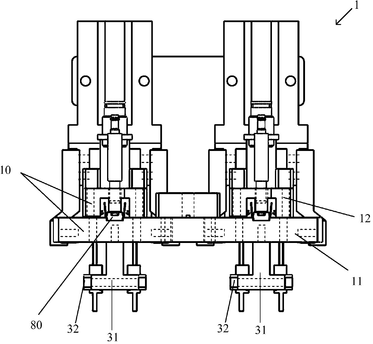
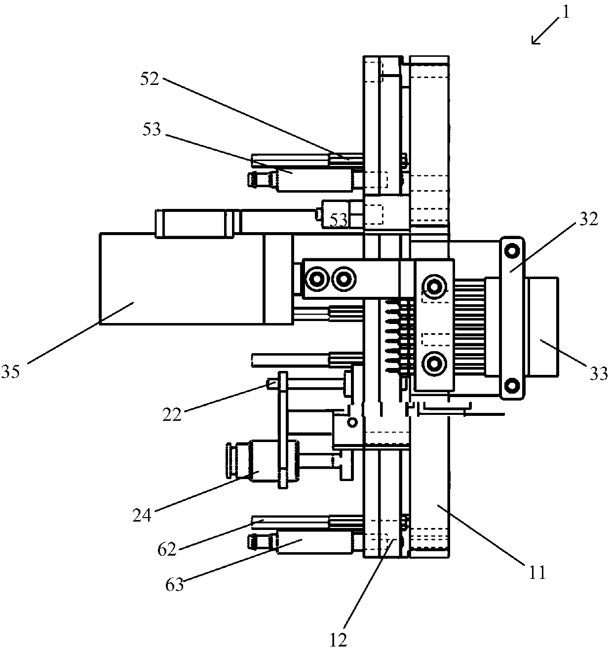
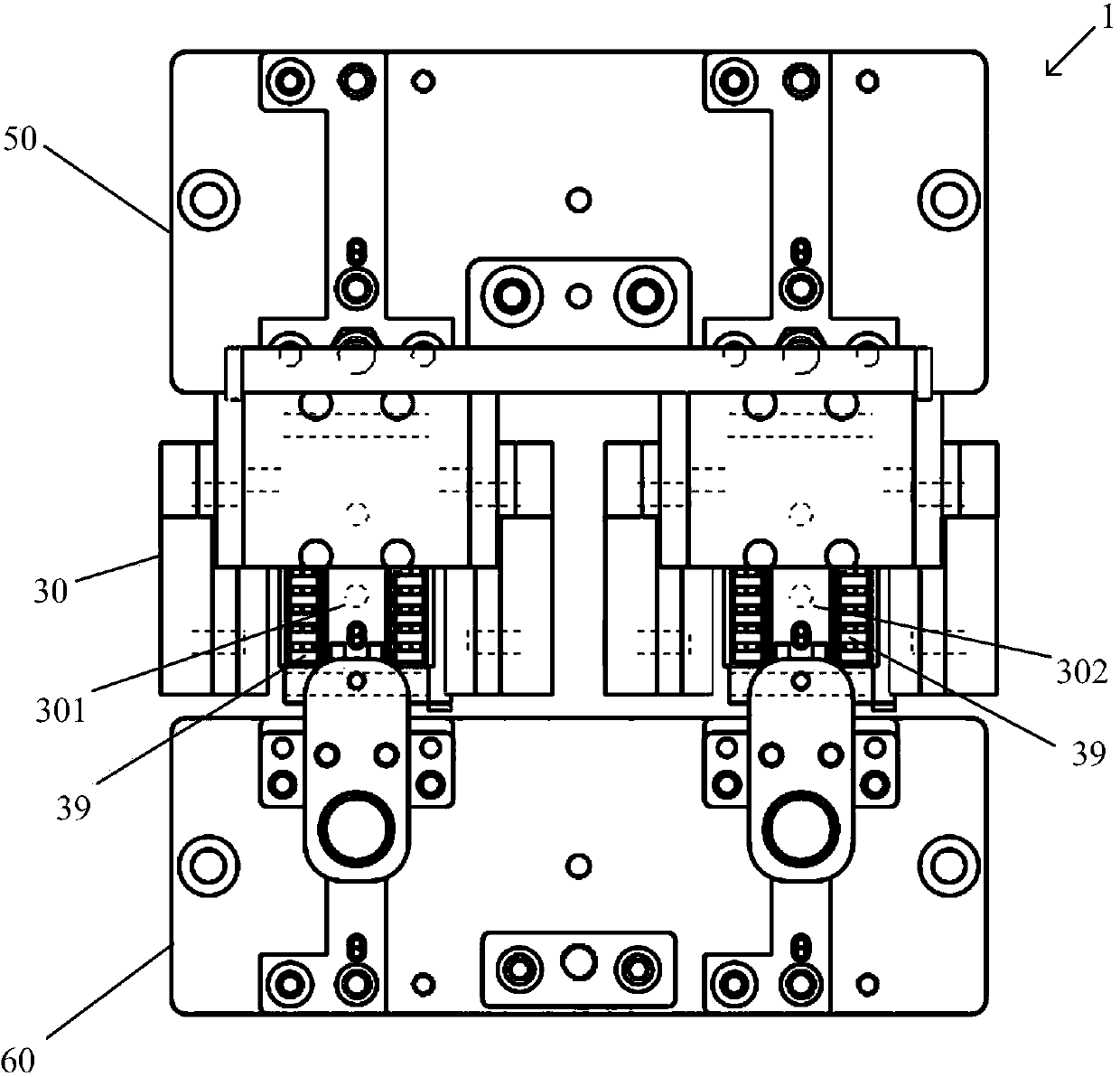
[0021] figure 1 , figure 2 and image 3 1 and 2 respectively show a top view, a side view and a front view of a part of the integrated circuit automatic test equipment 1 according to a preferred embodiment of the present invention. The illustrated automatic testing device 1 includes an upper temporary storage area 50 , a testing area 30 and a lower temporary storage area 60 ...


PUM


Abstract

The invention discloses an automatic testing device for an integrated circuit. The device comprises a testing region which is located on one part of a rail component and is used for testing an integrated circuit chip, wherein a gold finger fixing device used for fixing a gold finger and a blocking device used for blocking the integrated circuit chip from moving to the downstream place under the effect of gravity are arranged in the testing region; the blocking device comprises a blocking base, a blocking needle, a blocking air cylinder and a blocking shifting block; the blocking base is arranged on the rail component of the testing region; the blocking needle is capable of moving relative to the blocking base, and can be operated to abut against the lower side edge of the integrated circuit chip so as to block the integrated circuit chip; the blocking air cylinder is used for providing the actuating force for the blocking needle; the blocking shifting block is mounted on the blocking base in a pivoting way; one end of the blocking shifting block is abutted against the blocking air cylinder and is actuated by the blocking air cylinder; the other end of the blocking shifting block is matched with the blocking needle to move the blocking needle. By using the automatic testing device for the integrated circuit, the position of the blocking needle is precisely controlled, and the phenomenon that the chip is clamped or malposed is avoided.

Description

technical field [0001] The invention relates to the field of integrated circuit testing, in particular to an integrated circuit automatic testing device for automatically testing and classifying integrated circuit chips. Background technique [0002] In recent years, integrated circuits have been widely used in various fields, and the demand for integrated circuit products has grown exponentially. In order to adapt to the improvement of the production efficiency of integrated circuit products, there are currently existing technical means for automatic testing and classification of integrated circuits, which can save a lot of manpower and material resources. The existing integrated circuit automatic test device with the technical means of automatic test classification is suitable for the automatic test of integrated circuits in various packaging forms such as DIP, SOP, and SSOP. The integrated circuit automatic testing device generally includes an upper temporary storage are...

Claims


Application Information

Patent Timeline
IPC IPC(8): G01R31/28G01R1/02G01R1/04
Inventor 周望标
Owner HANGZHOU YOUWANG ELECTRONICS
Learn More