Method of manufacturing printed circuit board

A technology of printed circuit substrates and base substrates, which is applied in the direction of assembling printed circuits, circuits, and electrical components with electrical components. It can solve the problems of solder ball falling off and difficult to control the position with high precision, and achieve the effect of preventing falling off and preventing aggregation

Inactive Publication Date: 2014-03-12
SAMSUNG ELECTRO MECHANICS CO LTD
View PDF6 Cites 2 Cited by
  • Summary
  • Abstract
  • Description
  • Claims
  • Application Information

AI Technical Summary

Problems solved by technology

At this time, when the solder ball is placed on the bonding pad with a squeegee, the solder ball aggregates due to the flux remaining on the upper part of the mask, making it difficult to control the position with high precision.
In addition, when the solder ball is placed on the bonding pad and the flux is applied by printing, the flux may be rolled by the squeegee and the solder ball may fall off the bonding pad.

Method used


Image

  • Method of manufacturing printed circuit board
  • Method of manufacturing printed circuit board
  • Method of manufacturing printed circuit board

Examples


Embodiment Construction

[0035] The purpose, specific advantages, and novel features of the present invention will be further clarified by the following detailed description and preferred embodiments with reference to the accompanying drawings. In this specification, when assigning reference numerals to constituent elements in each drawing, care must be taken to attach the same numerals as much as possible even if the same constituent elements are shown in different drawings. In addition, terms such as "one side", "the other side", "first", and "second" are used to distinguish one component from other components, and the components are not limited by the terms. Hereinafter, when describing the present invention, detailed descriptions related to well-known technologies that may obscure the gist of the present invention will be omitted.

[0036] Hereinafter, preferred embodiments of the present invention will be described in detail with reference to the accompanying drawings.

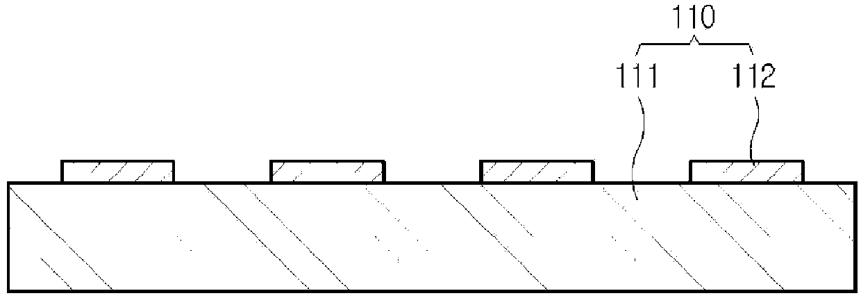
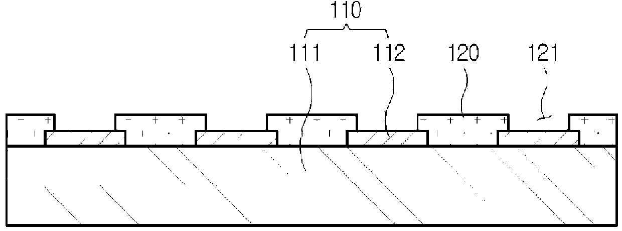
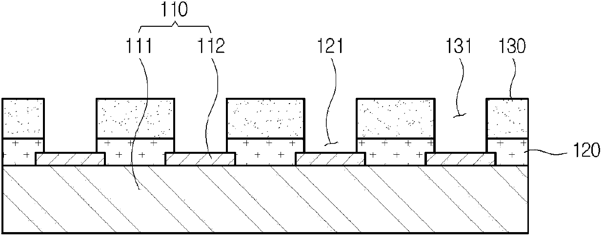
[0037] Manufacturing met...


PUM


Abstract

The present invention relates to a method of manufacturing printed circuit board. The method of manufacturing printed circuit board of the present invention includes the step of forming a solder resist in which a first opening is formed so that the step, and the upper portion of a bonding pad be exposed, the step of forming a mask in which a second opening is formed so that the upper portion of the bonding pad be exposed at the upper part of the solder resist, the step of setting up a solder ball at the upper part of the bonding pad, the step of coating a flux at the upper part of the solder ball, the step of performing the reflow and step of removing the mask, providing the base substrate including the bonding pad.

Description

technical field [0001] The invention relates to a preparation method of a printed circuit substrate. Background technique [0002] In recent years, with the development of electronic equipment, the demand for more functional and high-density electronic equipment has been increasing. However, due to the limited mounting area of ​​electronic components constituting the printed circuit board of the semiconductor package, regarding high-integration Research and development of printed circuit substrates is ongoing. Generally, in order to mount an electronic component on a printed circuit board, a method of forming a bump on a pad portion and electrically connecting the pad portion of the circuit layer and the electrode of the electronic component via the bump is used. In particular, miniaturized bumps are indispensable in order to correctly connect electronic components, which have recently tended to be miniaturized, with pads of printed circuit boards. [0003] Conventionally,...

Claims


Application Information

Patent Timeline
Patent Type & Authority Applications(China)
IPC IPC(8): H05K3/34
CPCH01L2224/11H01L23/12H05K3/34
Inventor 崔晋源柳然镐
Owner SAMSUNG ELECTRO MECHANICS CO LTD
Why Eureka
Try Eureka