Electroluminescent light emission device having an optical grating structure, and method for production thereof

A technology of light-emitting devices and lattice structures, which is applied in semiconductor/solid-state device manufacturing, electrical solid-state devices, electrical components, etc., and can solve problems such as light loss and loss

Active Publication Date: 2014-03-12
FRAUNHOFER GESELLSCHAFT ZUR FOERDERUNG DER ANGEWANDTEN FORSCHUNG EV
View PDF14 Cites 2 Cited by
  • Summary
  • Abstract
  • Description
  • Claims
  • Application Information

AI Technical Summary

Problems solved by technology

All in all, about 75%-80% of the light generated is lost due to these effects, and additionally by exciting plasmonic modes

Method used


Image

  • Electroluminescent light emission device having an optical grating structure, and method for production thereof
  • Electroluminescent light emission device having an optical grating structure, and method for production thereof
  • Electroluminescent light emission device having an optical grating structure, and method for production thereof

Examples


Embodiment Construction

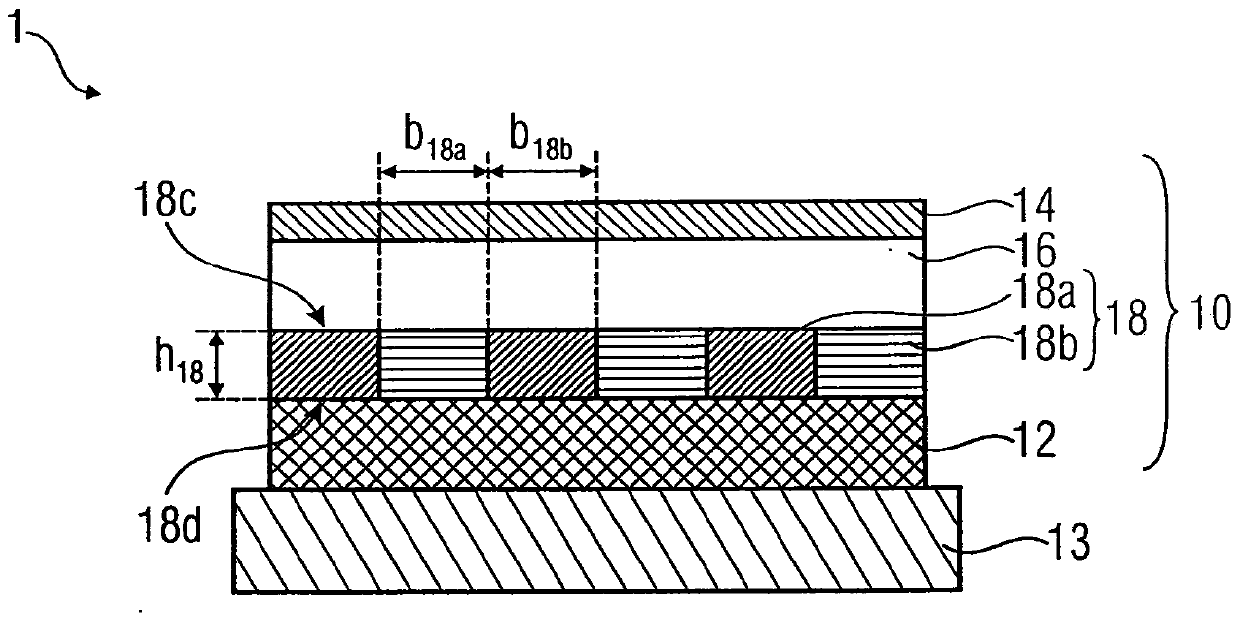
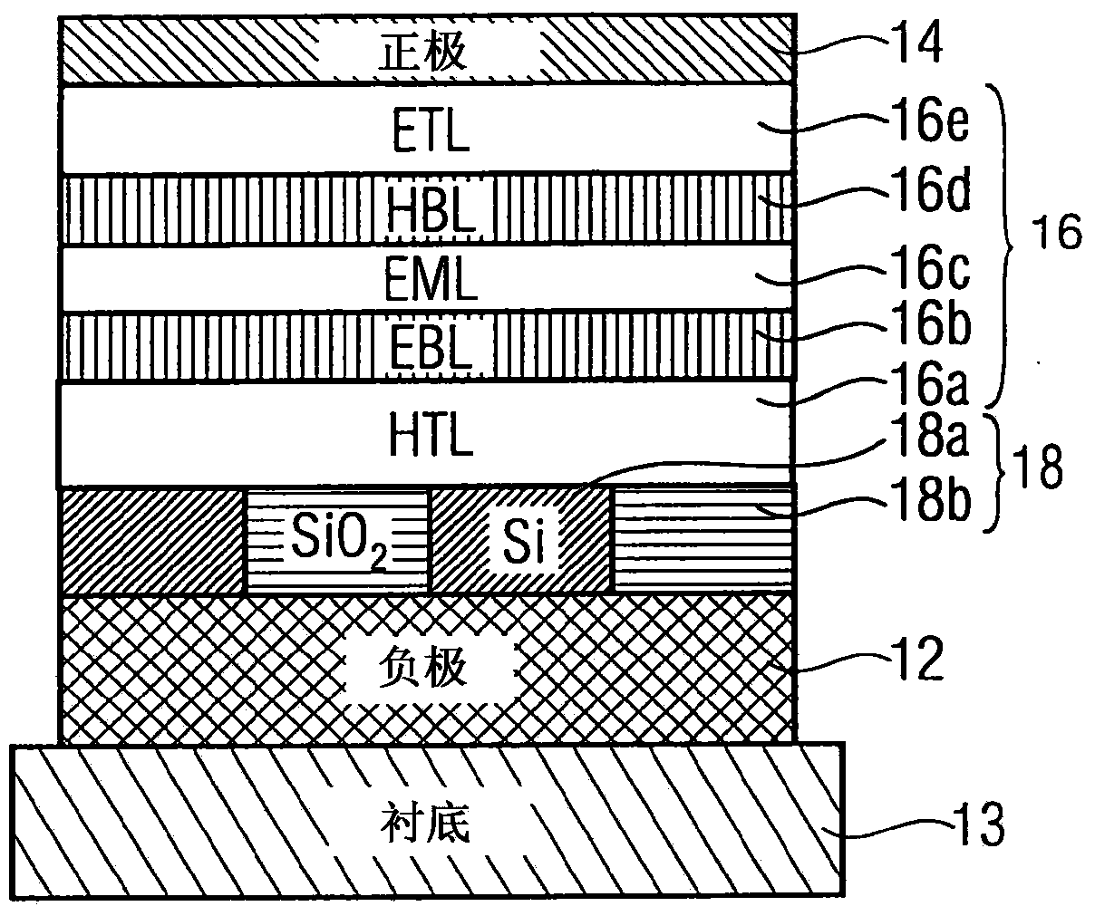
[0027] Before discussing the present invention in more detail below using the accompanying drawings, it is pointed out that the same elements, element structures and structures with the same function or the same effect are provided with the same reference numerals in different figures, so that elements and structures provided with the same reference numerals The descriptions presented in different embodiments of the present invention may be interchanged and shared.

[0028] will refer to figure 1 A planar electroluminescent device 1 according to a first embodiment of the present invention is described. specifically, figure 1 The layer arrangement 10 of the luminous means 1 applied onto a substrate 13 is shown. The layer arrangement 10 comprises a first electrode layer 12 and a second electrode layer 14, both of which comprise an electrically conductive material such as aluminum. A light-emitting layer 16 made of an organic material is arranged between the two electrode laye...


PUM


Abstract

A light emission device 1 comprises a substrate 13 and a layer arrangement 10 that has been applied to the substrate 13. The layer arrangement 10 has a first electrode layer 12 consisting of a conductive material and a second electrode layer 14 consisting of a conductive material. At least one light-emitting layer 16 consisting of an organic material is arranged between the first and second electrode layers 12 and 14. At least one intermediate layer 18 having an optical grating structure is arranged between the light-emitting layer 16 and one of the two electrode layers. A first main surface 18c of the intermediate layer 18 faces the light-emitting layer 16, said first main surface 18c of the intermediate layer having a planar design at least in the region of the optical grating structure within a tolerance range. At least regions of the intermediate layer 18 between the first main surface and a second main surface 18c and 18d thereof are conductive.

Description

technical field [0001] The present invention relates to an electroluminescent device comprising an optical lattice or grating for improving the coupling output of light, such as an organic light emitting diode or OLED, etc., and to a method of manufacturing the electroluminescent device. Background technique [0002] OLEDs are increasingly used in the field of lighting and in display technology. OLEDs' potentially high efficiency, achievable color spaces, and possible thinner form factors in particular contribute to this trend. [0003] The efficiency of OLEDs is determined by different factors, in high efficiency OLEDs especially the efficiency of outcoupling light limits the overall efficiency. Whereas light can be efficiently generated within the organic layers, only a fraction of the light can be coupled out of the OLED and used as useful light. Since the organic layer has a relatively high refractive index of about 1.7, most of the light in the organic light-emitting ...

Claims


Application Information

Patent Timeline
Patent Type & Authority Applications(China)
IPC IPC(8): H01L51/52
CPCH01L51/5275H01L51/52H01L51/5262H01L51/5048H10K50/14H10K50/80H10K50/858H10K50/85
Inventor 理查德·普法伊费尔卡斯滕·费泽乌韦·福格尔卡尔·里奥
Owner FRAUNHOFER GESELLSCHAFT ZUR FOERDERUNG DER ANGEWANDTEN FORSCHUNG EV
Why Eureka
Try Eureka