[0026] The specific implementations of the liquid crystal display panel and the display device provided by the embodiments of the present invention will be described in detail below with reference to the accompanying drawings.
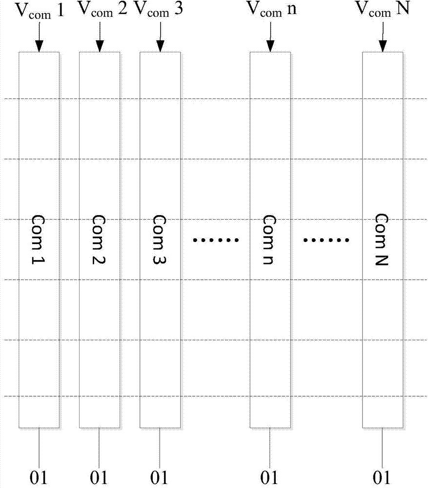
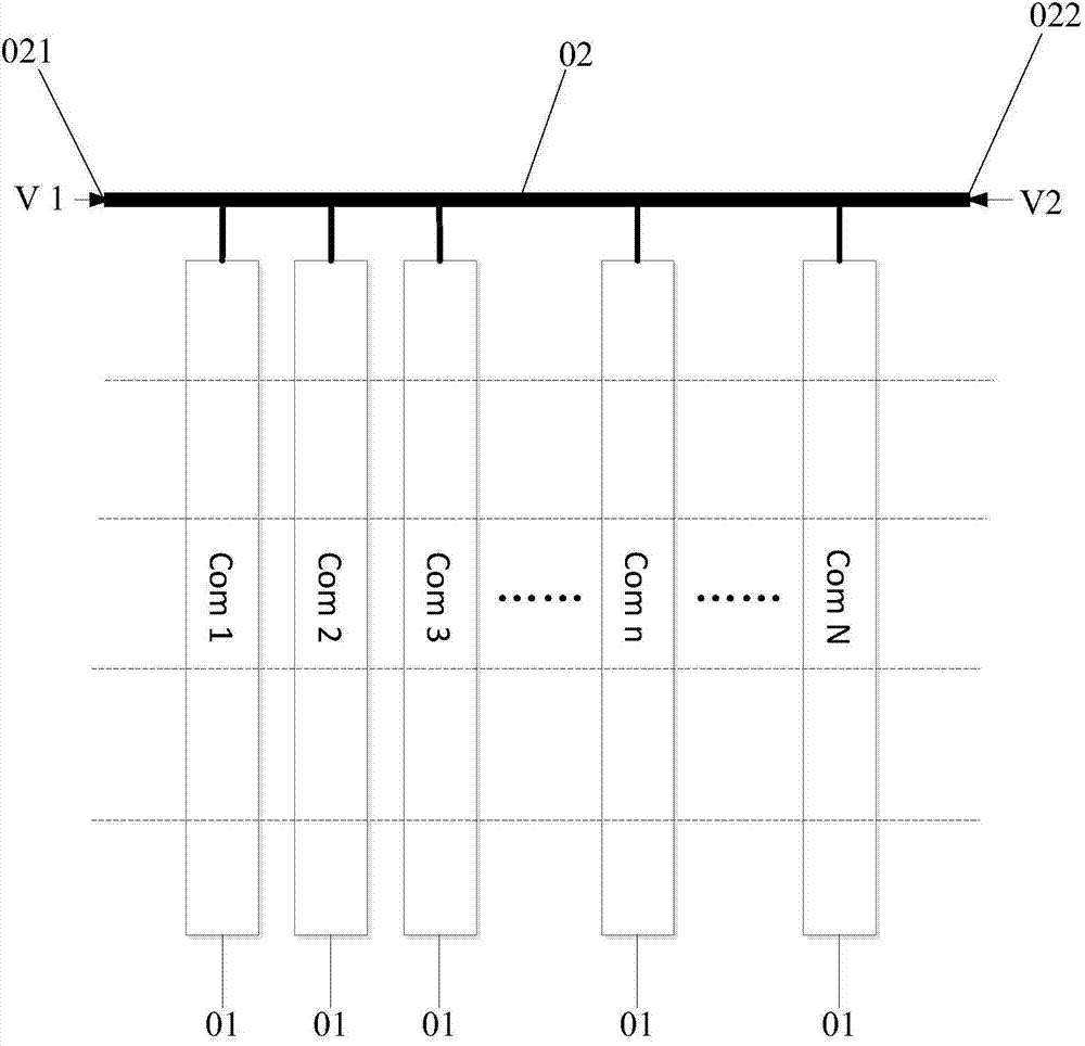
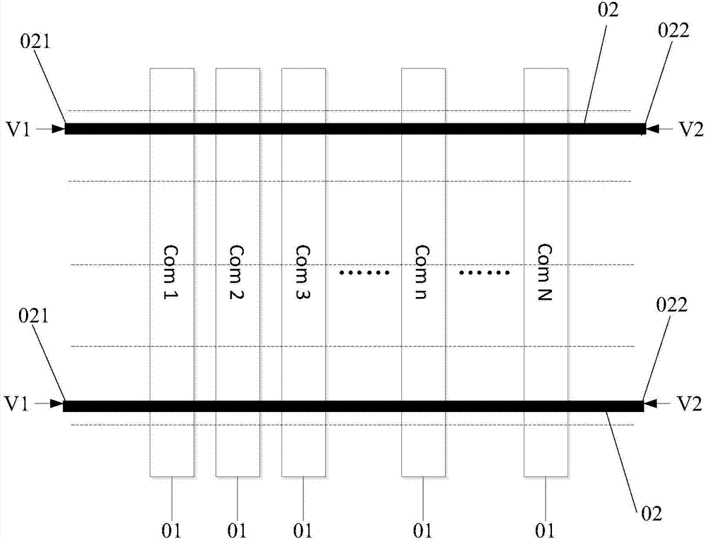
[0027] An embodiment of the present invention provides a liquid crystal display panel, comprising an array substrate with grid lines, and a counter substrate arranged opposite to the array substrate, and a common electrode is provided on the array substrate or the counter substrate;
[0028] like figure 1 shown, the common electrode is formed along the extension direction of the gate line ( figure 1 The dotted line in the middle is a gate line) composed of a plurality of sub-common electrodes 01 arranged side by side, and different common electrode signals V are respectively applied to each sub-common electrode 01 com n (n=1,2,...N, where N is the number of sub-common electrodes), and each common electrode signal V applied to each sub-common electrode com The voltage value of n gradually increases along the transmission direction of the gate signal on the gate line.
[0029] In the above-mentioned liquid crystal display panel provided by the embodiment of the present invention, since the common electrode is divided into a plurality of sub-common electrodes arranged side by side along the extension direction of the gate lines, compared with the existing liquid crystal display panel, the Applying different common electrode signals, in the above-mentioned liquid crystal display panel provided by the embodiment of the present invention, the voltage value of the common electrode signal applied on each sub-common electrode gradually increases along the transmission direction of the gate signal on the gate line, Therefore, the voltage on the sub-common electrode can compensate the voltage deviation ΔV of each pixel electrode in the entire liquid crystal display panel caused by the delay of the resistance and capacitance. P the inconsistency, thereby eliminating the due to ΔV P The inconsistency caused by the inconsistency of the picture flicker and other problems, and then improve the picture quality of the liquid crystal display panel.
[0030] In addition, since the common electrode signals applied to different sub-common electrodes are different, signal interference can be reduced, thereby improving the greening phenomenon of the liquid crystal display panel, thereby further improving the picture quality of the liquid crystal display panel.
[0031] Specifically, in the above-mentioned liquid crystal display panel provided by the embodiment of the present invention, such as figure 1 As shown, if the left end of the gate line in the figure is the gate signal input end, the common electrode signal V applied to each sub-common electrode 01 com n satisfies: V com 1 com 2 com N; if the right end of the gate line in the figure is the gate signal input end, then the common electrode signal V applied to each sub-common electrode 01 com n satisfies: V com 1>V com 2>…>V com N.
[0032] Preferably, in the above-mentioned liquid crystal display panel provided by the embodiment of the present invention, a plurality of sub-pixel units arranged in a matrix are generally arranged in the liquid crystal display panel; the orthographic projection of each sub-common electrode on the array substrate covers at least one column. Orthographic projection of sub-pixel units on the array substrate. That is, in the above-mentioned liquid crystal display panel provided by the embodiment of the present invention, the width of each sub-common electrode may be the width of one column of sub-pixel units or the width of multiple columns of sub-pixel units, which is not limited herein.
[0033] Further, in the above-mentioned liquid crystal display panel provided by the embodiment of the present invention, the shape of each sub-common electrode may be a rectangle, and of course the shape of the sub-common electrode may also be other shapes that can realize the solution of the present invention, which is not limited here.
[0034] Preferably, in the above-mentioned liquid crystal display panel provided by the embodiment of the present invention, the width of each sub-common electrode along the extending direction of the gate line can be set to be between the sub-common electrode and the gate signal input end of the gate line. distance is inversely proportional. This is because, generally in a liquid crystal display panel, along the gate signal transmission direction on the gate line, the farther from the gate signal input end of the gate line, the more serious the distortion of the gate signal, where each sub-common electrode is located The number of columns of the corresponding sub-pixel units can also be smaller, that is, the width of the sub-common electrodes can be smaller, so that more sub-common electrodes applied with different common electrode signals can be set here to compensate for the gate signal. The voltage deviation ΔV of the pixel electrode caused by the serious distortion P Inconsistency; the closer to the gate signal input end of the gate line, the less likely the gate signal is distorted, and the number of columns of sub-pixel units corresponding to each sub-common electrode here can also be more, that is, the sub-common electrode. The width can be larger, so as to ensure that the voltage deviation ΔV of the pixel electrode can be compensated PIn the case of inconsistency, the manufacturing process difficulty of the common electrode here is reduced. Specifically, in the liquid crystal display panel, the width of each sub-common electrode may be determined according to the actually required balance effect of the voltage value of the common electrode, which is not limited herein.
[0035] Preferably, in order to simplify the manufacturing process, in the above-mentioned liquid crystal display panel provided by the embodiment of the present invention, such as figure 1 As shown, the sub-common electrodes 01 can also be set to have the same width along the extension direction of the gate lines.
[0036] Since the delay (Delay) that occurs when the gate signal in the liquid crystal display panel is transmitted on the gate line changes linearly, in the above-mentioned liquid crystal display panel provided by the embodiment of the present invention, it is possible to pass the wiring in the liquid crystal display panel The resistors are used to generate different linear voltages, so that different common electrode signals can be respectively applied to each sub-common electrode, and the voltage value of each common electrode signal applied to each sub-common electrode is along the line of the gate signal on the gate line. The direction of transmission increases gradually.
[0037] Therefore, in the specific implementation, it can be Figure 2a and Figure 2b The shown trace 02 connects the sub-common electrodes 01 in series with each other, and different common electrode signals are respectively applied to both ends of the trace, that is, the first common electrode signal V1 is applied to the first end 021 of the trace, and the A second common electrode signal V2 is applied to the second end 022 of the trace, and there is a voltage difference between the first common electrode signal V1 and the second common electrode signal V2, so as to apply different common electrode signals to each sub-common electrode respectively.
[0038] The specific principle is that different signals are applied at both ends of the trace 02, so that there is a voltage difference between the two ends of the trace. Due to the existence of the resistance of the trace itself, the voltage difference can be distributed to the resistance of the trace, thus Different positions on the trace have different voltages, and each sub-common electrode 01 is connected in series to different positions on the trace 02, so that the voltages at different positions on the trace 02 are respectively applied to the position connected to the trace 02. sub-common electrode 01.
[0039] Further, in specific implementation, such as Figure 2a and Figure 2b As shown (the dotted line in the figure is the gate line), if the left end of the gate line in the figure is the gate signal input terminal, the voltage value of the first common electrode signal V1 should be smaller than the voltage value of the second common electrode signal V2, that is, the voltage value of the first common electrode signal V2 is The voltage value of each point on the line 02 gradually increases along the first end 021 to the second end 022 of the line 02; if the right end of the gate line in the figure is the gate signal input end, the voltage of the first common electrode signal V1 The value should be greater than the voltage value of the second common electrode signal V2 , that is, the voltage value of each point on the trace 02 gradually decreases along the first end 021 to the second end 022 of the trace 02 .
[0040] Specifically, in the above-mentioned liquid crystal display panel provided in the embodiment of the present invention, the selection of the voltage values of the first common electrode signal V1 and the second common electrode signal V2 can be set according to actual needs. When the display effect is displayed, the voltage values of the first common electrode signal and the second common electrode signal are determined by the voltage values actually required by the first end and the second end of the wiring.
[0041] Specifically, in the above-mentioned liquid crystal display panel mentioned in the embodiment of the present invention, such as Figure 2a As shown, there can be one line connecting all the sub-common electrodes in series. Of course, there can also be multiple lines connecting all the sub-common electrodes in series, such as Figure 2b Further, in the specific implementation, in order to ensure the aperture ratio of the liquid crystal display panel, the wiring is generally arranged in the non-display area of the liquid crystal display panel, which is not limited here.
[0042] Preferably, in the above-mentioned liquid crystal display panel mentioned in the embodiment of the present invention, such as Figure 2a and Figure 2b As shown, the resistance value of the trace 02 between two adjacent sub-common electrodes 01 is proportional to the distance between the center points of the two adjacent sub-common electrodes 01 . In specific implementation, the sub-common electrode 01 is generally rectangular, and the center point of the sub-common electrode is the intersection of two diagonal lines of the rectangle. The greater the distance between the center points of two adjacent sub-common electrodes 01, the longer the length of the wiring used to connect the two adjacent sub-common electrodes 01, so as to connect the wiring between the two adjacent sub-common electrodes 01 The greater the resistance is.
[0043] Preferably, in the specific implementation, in the above-mentioned liquid crystal display panel provided by the embodiment of the present invention, such as Figure 2a and Figure 2b As shown, the extension direction of the trace 02 can be the same as the extension direction of the gate line ( Figure 2a and Figure 2b The dotted line is the grid line) is the same.
[0044] Further, in order to simplify the process steps and save the production cost, in the above-mentioned liquid crystal display panel provided by the embodiment of the present invention, the wiring is set to the same layer and the same material as the gate line; or the wiring is set to the same layer and the same layer as the data line. material. In this way, during the preparation, the wiring and the gate line or the data line can be prepared in the same layer, so that it is not necessary to add a new preparation process, and only needs to change the pattern of the corresponding film layer.
[0045] Further, in the above-mentioned liquid crystal display panel mentioned in the embodiment of the present invention, such as image 3 As shown, the first common electrode signal and the second common electrode signal can be applied to the first end 021 and the second end 022 of the wiring 02 through the driving chip (IC) 03 of the liquid crystal display panel, respectively. In specific implementation, a first signal output terminal 031 and a second signal output terminal 032 for outputting a common electrode signal are set in the driver chip 03, and the first signal output terminal 031 is connected to the first terminal 021 of the wiring 02 for use in The first common electrode signal is output to the first end 021 of the trace 02 ; the second signal output terminal 032 is connected to the second end 022 of the trace, and is used to output the second common electrode signal to the second end 022 of the trace 02 .
[0046] Specifically, the specific structure of the above-mentioned driving chip is in the prior art, and details are not described here.
[0047] Based on the same inventive concept, an embodiment of the present invention also provides a display device, including the above-mentioned liquid crystal display panel provided by the embodiment of the present invention, and the display device may be: a mobile phone, a tablet computer, a TV, a monitor, a notebook computer, a digital photo frame , navigator and any other product or component with display function. For the implementation of the display device, reference may be made to the above-mentioned embodiments of the liquid crystal display panel, and repeated descriptions will not be repeated.
[0048] An embodiment of the present invention provides a liquid crystal display panel and a display device. In the liquid crystal display panel, since the common electrode is divided into a plurality of sub-common electrodes arranged side by side along the extension direction of the grid lines, it is different from the existing liquid crystal display panel. Compared with the panel, different common electrode signals can be applied to each sub-common electrode. In the above-mentioned liquid crystal display panel provided by the embodiment of the present invention, the voltage value of the common electrode signal applied to each sub-common electrode is along the grid line. The transmission direction of the polar signal is gradually increased, so the voltage on the sub-common electrode can compensate the voltage deviation ΔV of each pixel electrode in the entire liquid crystal display panel caused by the delay of the resistance and capacitance. P the inconsistency, thereby eliminating the due to ΔV P The inconsistency caused by the inconsistency of the picture flicker and other problems, and then improve the picture quality of the liquid crystal display panel. In addition, since the common electrode signals applied to different sub-common electrodes are different, signal interference can be reduced, thereby improving the greening phenomenon of the liquid crystal display panel, thereby further improving the picture quality of the liquid crystal display panel.
[0049] It will be apparent to those skilled in the art that various modifications and variations can be made in the present invention without departing from the spirit and scope of the invention. Thus, provided that these modifications and variations of the present invention fall within the scope of the claims of the present invention and their equivalents, the present invention is also intended to include these modifications and variations.