A common anode micro-display pixel driving circuit and driving method

A pixel drive circuit and common anode technology, applied in static indicators, instruments, etc., can solve the problems of difficult to improve the accuracy of micro-displays, and achieve the effects of eliminating screen flicker, wide adjustable range, and saving area

Active Publication Date: 2021-03-30
NANJING GUOZHAO OPTOELECTRONICS TECH CO LTD
View PDF10 Cites 0 Cited by
  • Summary
  • Abstract
  • Description
  • Claims
  • Application Information

AI Technical Summary

Problems solved by technology

[0003] The purpose of the present invention aims at the problem that the existing micro-display precision is difficult to improve, and designs a common anode micro-display pixel driving circuit and driving method based on silicon-based micro-display driving circuit

Method used


Image

  • A common anode micro-display pixel driving circuit and driving method
  • A common anode micro-display pixel driving circuit and driving method
  • A common anode micro-display pixel driving circuit and driving method

Examples


Embodiment 1

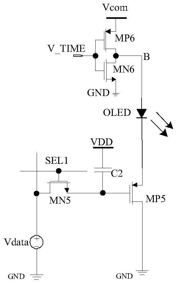
[0020] Such as figure 1 shown.

[0021] A common anode micro-display pixel drive circuit, the drain of the N-type MOS transistor MN5 is connected to the positive terminal of the input voltage source Vdata, the source of the N-type MOS transistor MN5 is connected to one end of the capacitor C2, and the gate of the P-type MOS transistor MP5 connected. The gate of the N-type MOS transistor MN5 is connected to the external control signal SEL1. The negative end of the voltage source Vdata is connected to the ground GND. The source of the P-type MOS transistor MP5 is connected to the cathode of the OLED, and the drain of the P-type MOS transistor MP5 is connected to GND. The OLED anode is connected to point B with the drain of the P-type MOS transistor MP6 and the drain of the N-type MOS transistor MN6. The source of the P-type MOS transistor MP6 is connected to VCOM, the gate of the P-type MOS transistor MP6 and the gate of the N-type MOS transistor MN6 are connected to V_TIME,...

Embodiment 2

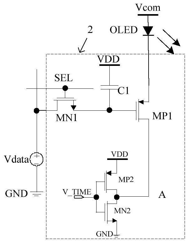
[0026] Such as image 3 .

[0027] A common anode micro-display pixel driving circuit is composed of a specific pixel circuit in the dotted line frame 2, an external voltage source Vdata, and an external OLED. The drain of the N-type MOS transistor MN1 is connected to the positive terminal of the input voltage source Vdata, and the source of the N-type MOS transistor MN1 is connected to one end of the capacitor C1 and the gate of the P-type MOS transistor MP1. The gate of the N-type MOS transistor MN1 is connected to the external control signal SEL. The negative end of the voltage source Vdata is connected to the ground GND. The source of the P-type MOS transistor MP1 is connected to the cathode of the OLED, and the anode of the OLED is connected to the VCOM voltage. The drain of the P-type MOS transistor MP1 is connected to the drain of the P-type MOS transistor MP2 and the drain of the N-type MOS transistor MN2 at point A. The source of the P-type MOS transistor MP2 is c...

Embodiment 3

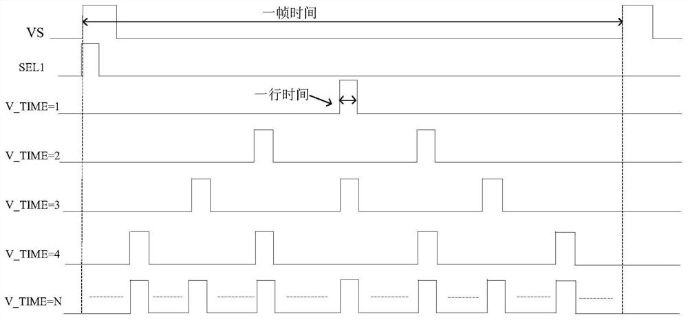
[0032] A common anode micro-display pixel driving method, using PFM control mode, when V_TIME=N, after the field synchronization signal becomes high level, N V_TIME high pulses are generated on average within one field time, and the width of one pulse is one line time , MN6 is turned on when the V_TIME pulse is at a high level, the voltage at point B is equal to the GND voltage, MP5 is turned off, and after the V_TIME pulse becomes low level, the voltage at point B is equal to the VCOM voltage, the current generated by MP5 flows through the OLED, and the OLED starts Lighting; such a cycle, OLED from extinguishing to luminous and then to luminous to extinguished, thus realizing the precise control of the light emitting time of the OLED device, in the case of a fixed pulse width, the precise adjustment of the brightness of the OLED light is realized by adjusting the pulse frequency. The VPLUSE signal is divided into N levels, and regulates the common anode voltage VCOM or the pow...


PUM


Abstract

A common anode micro-display pixel drive circuit and drive method, characterized in that the drive circuit includes a drive tube MP5, a switch tube MN5, a switch tube MP6, a switch tube MN6, and a storage capacitor C2. When V_TIME=N, after the field synchronization signal becomes high level, N V_TIME high pulses are generated on average in one field, and the width of one pulse is one line time. MN6 is turned on during the high level of V_TIME pulse, point B The voltage is equal to the GND voltage, MP5 is turned off, and after the V_TIME pulse becomes low level, the voltage at point B is equal to the VCOM voltage, the current generated by MP5 flows through the OLED, and the OLED starts to emit light. The light-emitting time is controlled by the V_TIME pulse to realize brightness adjustment. The pixel circuit of the present invention can realize an N-level dimming range without affecting the light emitting characteristics of the OLED.

Description

technical field [0001] The invention relates to the field of microelectronics and display technology, in particular to a common anode silicon-based micro-display drive circuit, in particular to a common-anode micro-display pixel drive circuit and a drive method. Background technique [0002] Micro-display technology is an emerging display technology, which realizes the combination of display technology and silicon-based integrated circuit technology. Its display technology has experienced CRT microdisplays, LCD microdisplays, liquid crystal on silicon (LCoS) microdisplays, silicon-on-organic light-emitting diode (OLED-on-Silicon) microdisplays, Micro-LED microdisplays, etc. People's requirements for display quality are getting higher and higher. Among them, the pixel circuit directly drives the OLED and LED to emit light. Traditional scanning imaging adopts the method of analog driving to adjust the grayscale and brightness of pixels by controlling the magnitude of the vol...

Claims


Application Information

Patent Timeline
Patent Type & Authority Patents(China)
IPC IPC(8): G09G3/3225G09G3/3258
CPCG09G3/3225G09G3/3258G09G2310/0264
Inventor 张白雪秦昌兵陈啟宏徐亭亭杨建兵
Owner NANJING GUOZHAO OPTOELECTRONICS TECH CO LTD
Why Eureka
Try Eureka