Adhesive tape joining method and adhesive tape joining apparatus

A technology of sticking device and adhesive tape, which is applied in the manufacturing of electrical components, electric solid-state devices, semiconductor/solid-state devices, etc., which can solve the problems of chip flying, peeling, and uneven tension of the adhesive tape.

Inactive Publication Date: 2014-03-26
NITTO DENKO CORP
View PDF5 Cites 2 Cited by
  • Summary
  • Abstract
  • Description
  • Claims
  • Application Information

AI Technical Summary

Problems solved by technology

In the case of pasting the adhesive tape on the back surface of the wafer by the conventional method, the adhesive tape temporarily pasted on the wafer may be stuck between the flat surface at the center of the wafer and the ring-shaped protrusion due to slight uneven tension. Problems such as peeling of the corners
That is, if the adhesive tape is peeled off, there will be a problem that the separated chips will be scattered during the dicing process.

Method used


Image

  • Adhesive tape joining method and adhesive tape joining apparatus
  • Adhesive tape joining method and adhesive tape joining apparatus
  • Adhesive tape joining method and adhesive tape joining apparatus

Examples


Embodiment Construction

[0031] In order to explain the invention, several embodiments considered to be suitable at present are shown in the drawings, but it is understood that the present invention is not limited to the structures and methods shown in the drawings.

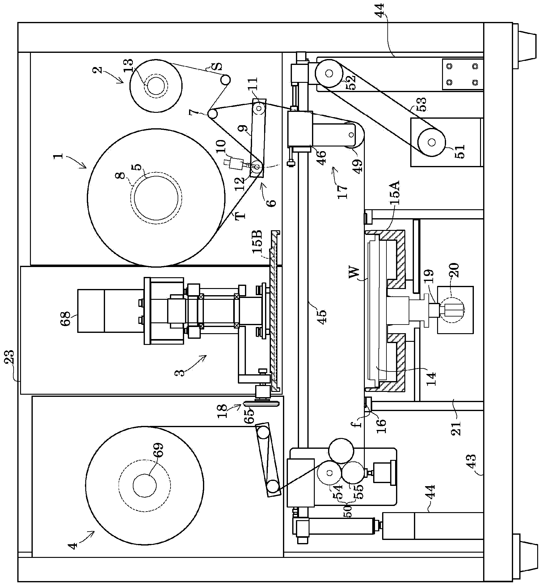
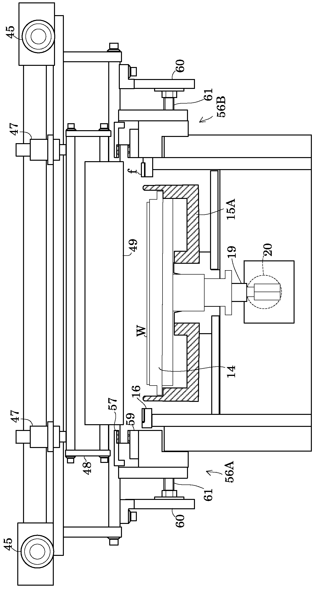
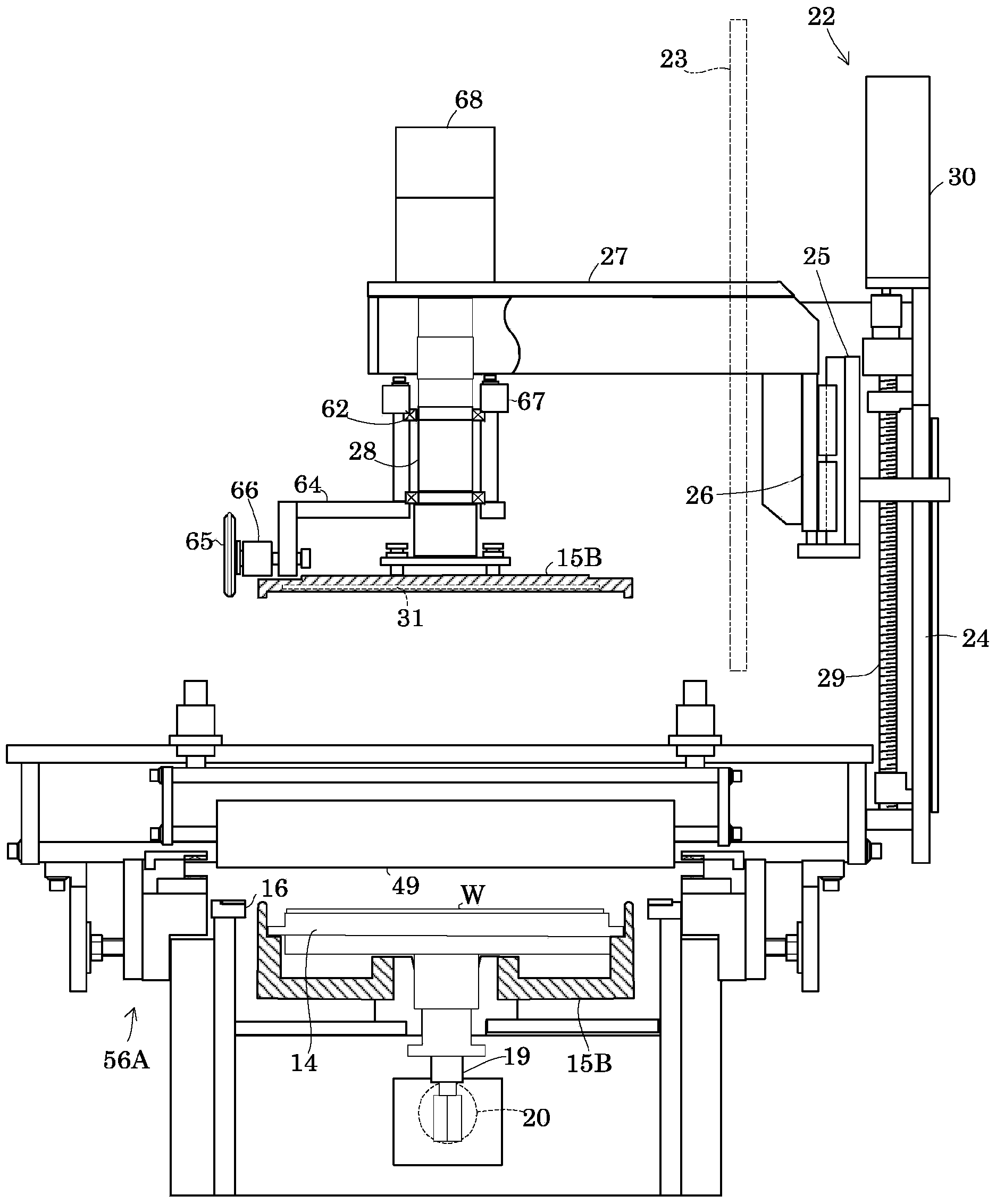
[0032] Hereinafter, an embodiment of the present invention will be described with reference to the drawings. In addition, if Figure 13 ~ Figure 15 As shown, the semiconductor wafer (hereinafter, simply referred to as “wafer”) used in this embodiment is a wafer in which a protective tape PT is pasted on the surface on which the circuit is formed to protect the surface and has undergone backgrinding. Using a wafer processed into a shape in which the back surface of the wafer is ground (background) so that the outer peripheral portion is left about 2 mm in the radial direction, a flat concave portion b is formed on the back surface, and along the back surface The ring-shaped convex part r remains on the outer periphery. For example, the ...


PUM


Abstract

The invention provides an adhesive tape joining method and an adhesive tape joining apparatus. An adhesive tape is joined onto an annular frame in a state that a tensile force is applied onto the adhesive tape in the length and width directions of the adhesive tape, wherein the adhesive tape is band-shaped and the self-width of the adhesive tape is greater than the outline width of the annular frame. A pair of covers are used to clamp the adhesive tape between the annular frame and a semiconductor wafer, thereby forming a chamber. The pressure of one space formed by separation via the adhesive tape (T) and accommodating the wafer is decreased to be lower than the pressure of the other space, so that the adhesive tape (T) is joined onto an annular convex part formed in the periphery of the wafer and a flat plane in the inner side of the annular convex part.

Description

technical field [0001] The present invention relates to attaching an adhesive tape for support to the back surface of a semiconductor wafer (hereinafter, appropriately referred to as a "wafer") placed in the center of a ring frame and to the ring frame to make the semiconductor wafer and the ring frame An adhesive tape pasting method and an adhesive tape pasting device integrated with a ring frame. Background technique [0002] In order to prevent the chip components separated from the wafer from flying during the dicing process, a method has been proposed in which the adhesive tape for support is adhered to the back surface of the wafer when the adhesive tape for support is attached to the wafer. Here, in order to achieve miniaturization of the device used to implement the method, instead of using a sticking roller, an adhesive tape is used to separate the chamber composed of a pair of upper and lower covers to form two spaces, and to make one space The adhesive tape is at...

Claims


Application Information

Patent Timeline
Patent Type & Authority Applications(China)
IPC IPC(8): H01L21/00H01L21/02
CPCH01L21/6836H01L2221/68327H01L21/566H01L21/67132
Inventor 奥野长平山本雅之
Owner NITTO DENKO CORP
Why Eureka
Try Eureka