Semiconductor device and method of manufacturing same

A manufacturing method and semiconductor technology, applied in semiconductor/solid-state device manufacturing, semiconductor devices, electrical components, etc., can solve problems such as deviation in shape and large size

Inactive Publication Date: 2014-03-26
KK TOSHIBA
View PDF5 Cites 2 Cited by
  • Summary
  • Abstract
  • Description
  • Claims
  • Application Information

AI Technical Summary

Problems solved by technology

However, the conventional resistive field plate structure has variations in its shape, and its size is large

Method used


Image

  • Semiconductor device and method of manufacturing same
  • Semiconductor device and method of manufacturing same
  • Semiconductor device and method of manufacturing same

Examples


Embodiment Construction

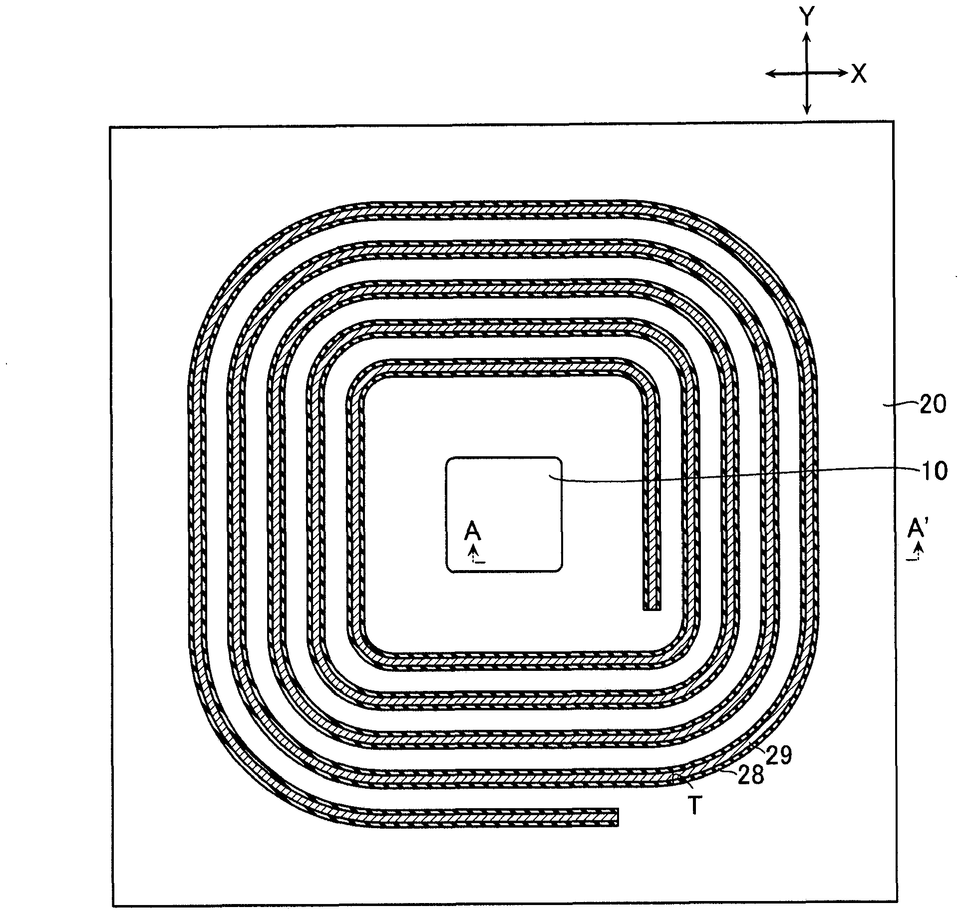
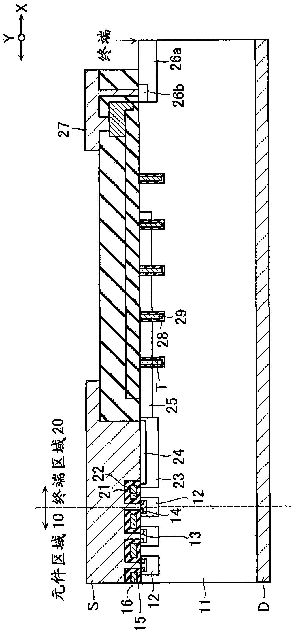
[0012] Below, refer to figure 1 and figure 2 The semiconductor device according to the embodiment will be described. figure 1 is a top view showing the semiconductor device according to the embodiment, figure 2 yes figure 1 A-A' sectional view of . also, figure 1 Only the element region 10 , termination region 20 , trench T, insulating layer 28 , and field plate conductive layer 29 to be described later are shown, and other structures are omitted.

[0013] Such as figure 1 As shown, the semiconductor device according to the embodiment includes: an element region 10 forming a semiconductor element (for example, a vertical power MOSFET) and a terminal region 20 surrounding the element region 10 and forming a resistive field plate structure. In addition, as an example, assume that the boundary between the element region 10 and the terminal region 20 in this embodiment is the center of the p-type base layer 12 located at the outermost end ( figure 2 ).

[0014] Next, th...


PUM


Abstract

The invention provides a semiconductor device and a method of manufacturing same. The semiconductor device includes an element region and an end region, the element region having a semiconductor element formed therein, and the end region surrounding the element region. The semiconductor device includes a semiconductor substrate, a trench, an insulating layer, and a field plate conductive layer. The trench is formed in the semiconductor substrate so as to surround the element region in the end region. The field plate conductive layer is formed in the trench via the insulating layer.

Description

[0001] (Cross-reference to related application) [0002] This application is based on and claims priority from prior Japanese Patent Application No. 2012-206195 filed on September 19, 2012, the entire contents of which are hereby incorporated by reference. technical field [0003] This embodiment mode relates to a semiconductor device and a manufacturing method thereof. Background technique [0004] In the terminal region surrounding the element region where the semiconductor element is formed, various structures are used to maintain a breakdown voltage by alleviating electric field concentration. As one of them, a resistive field plate (RFE: Resistive Field Plate) structure is known. However, conventional resistive field plate structures vary in shape and are large in size. Contents of the invention [0005] Embodiments of the present invention provide a semiconductor device in which concentration of an electric field in a termination region is alleviated, and a method ...

Claims


Application Information

Patent Timeline
Patent Type & Authority Applications(China)
IPC IPC(8): H01L29/40H01L29/06H01L29/10H01L29/78H01L21/28H01L21/336
CPCH01L29/0615H01L29/7393H01L29/402H01L29/66712H01L21/4814H01L29/0619H01L29/7395H01L29/0607H01L29/7811H01L29/407H01L29/0638
Inventor 泉泽优小野昇太郎大田浩史山下浩明
Owner KK TOSHIBA
Why Eureka
Try Eureka