

Semiconductor device
A semiconductor and housing technology, applied in the direction of semiconductor devices, semiconductor/solid-state device components, electric solid-state devices, etc., can solve the problem of reducing the self-inductance of semiconductor devices, and achieve the effect of reducing the self-inductance and easing the concentration of magnetic flux.
- Summary
- Abstract
- Description
- Claims
- Application Information
AI Technical Summary
Problems solved by technology
Method used
Image

Examples
Embodiment approach 1
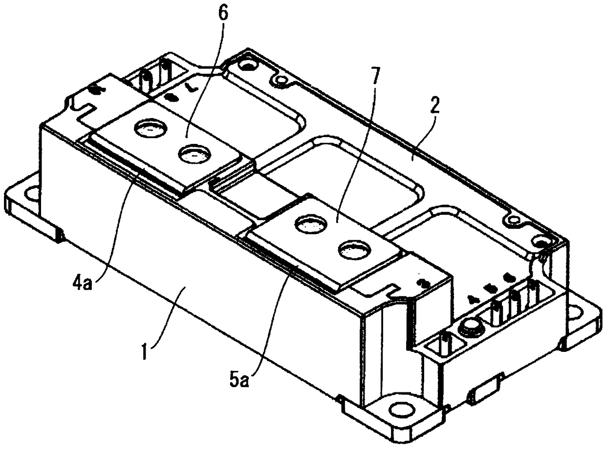
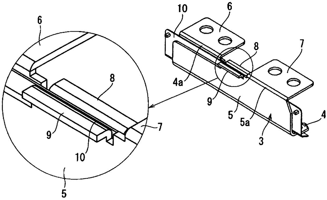
[0026] Hereinafter, the first embodiment of the present invention will be described with reference to the drawings. figure 1 Is a perspective view of the semiconductor device according to the first embodiment, figure 2 It is a perspective view of the parallel plate 3 and the electrodes 6 and 7 of the semiconductor device according to the first embodiment.
[0027] Such as figure 1 with figure 2 As shown, the semiconductor device is a power module such as an IGBT module or a SiC module, and has a resin case 1, a parallel flat plate 3, and electrodes 6, 7. The resin case 1 is formed in a box shape, and a semiconductor element (not shown) is accommodated inside. Regarding the resin case 1, the upper surface of the front portion is formed to be located at a higher height position than the upper surface of the rear portion. A cover 2 is arranged at the upper end of the rear part of the resin case 1, and the cover 2 forms the upper surface of the rear part of the resin case 1.
[0028...
Embodiment approach 2
[0043] Next, the semiconductor device according to Embodiment 2 will be described. Image 6 It is a perspective view of the parallel plate 3 and the electrodes 6 and 7 of the semiconductor device according to the second embodiment. In addition, in the second embodiment, the same components as those described in the first embodiment are assigned the same reference numerals, and the description is omitted.
[0044] Such as Image 6 As shown, in Embodiment 2, the distance between the upper portions of the parallel plate 3 located between the two electrode lead-out portions 4a, 5a is greater than the distance between the portions other than the upper portion located between the two electrode lead-out portions 4a, 5a. width. More specifically, the upper part of the plate 5 that constitutes the parallel plate 3 between the electrode lead-out parts 4a, 5a is provided with a projecting part 12 projecting outward, so that the parallel plate 3 is located between the electrode lead-out part...
Embodiment approach 3
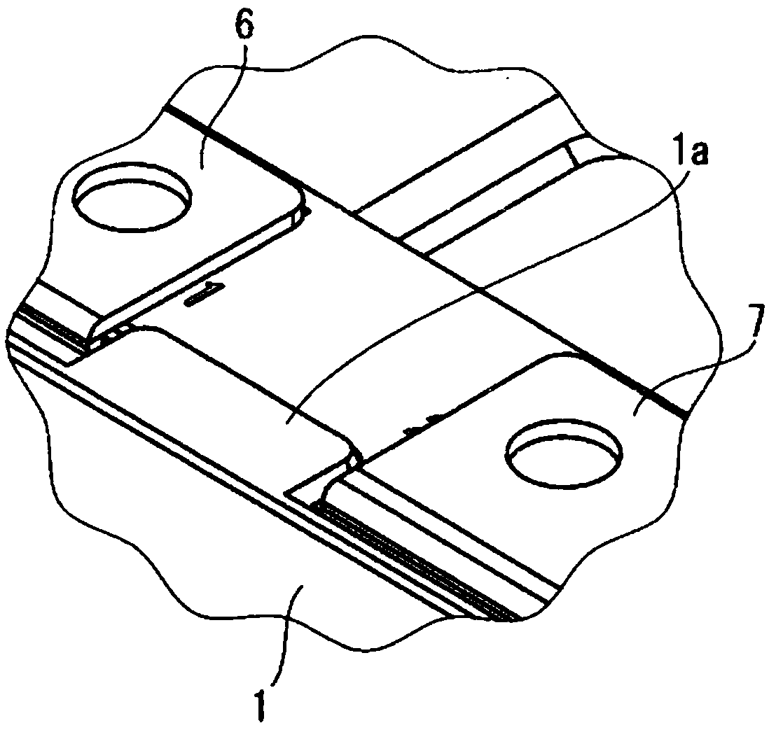
[0049] Next, a semiconductor device according to Embodiment 3 will be described. Figure 7 It is a perspective view of the parallel plate 3 and the electrodes 6, 7 of the semiconductor device according to the third embodiment, Picture 8 It is a plan view showing a portion of the parallel flat plate 3 of the semiconductor device according to the third embodiment located between the electrode lead-out portions 4a and 5a. In addition, in Embodiment 3, the same components as those described in Embodiments 1 and 2 are denoted by the same reference numerals, and descriptions thereof will be omitted.
[0050] Such as Figure 7 , Picture 8 As shown, in Embodiment 3, the extension 11 is provided on the upper part of the plate 4 between the electrode lead-out parts 4a, 5a, and the extension 12 is provided on the plate 5 between the electrode lead-out parts 4a, 5a. Upper part. Therefore, the interval between the upper portions of the parallel plate 3 located between the electrode lead-out...
PUM
 Abstract
Description
Claims
Application Information