Light-emitting diode device and manufacturing method thereof

A technology for a light-emitting diode and a manufacturing method, which is applied to semiconductor devices, electrical components, circuits, etc., can solve the problems of non-electrical connection of light-emitting chips, false welding of the number of contacts, and reduced reliability of light-emitting diode modules.

Inactive Publication Date: 2014-03-26
LEXTAR ELECTRONICS CORP
View PDF3 Cites 0 Cited by
  • Summary
  • Abstract
  • Description
  • Claims
  • Application Information

AI Technical Summary

Problems solved by technology

[0003] In this way, the light-emitting diode module will form at least four soldered joints, not only the cost of the wire is high, but also false welding may occur due to the large number of joints, so that the light-emitting chip may not be electrically connected to the base, resulting in the failure of the light-emitting diode module. Reduced reliability

Method used


Image

  • Light-emitting diode device and manufacturing method thereof
  • Light-emitting diode device and manufacturing method thereof
  • Light-emitting diode device and manufacturing method thereof

Examples


Embodiment Construction

[0060] A number of embodiments of the present invention will be disclosed below with the accompanying drawings. For the sake of clarity, many practical details will be described together in the following description. It should be understood, however, that these practical details should not be used to limit the invention. That is, in some embodiments of the present invention, these practical details are unnecessary. In addition, for the sake of simplifying the drawings, some known and conventional structures and elements will be shown in a simple and schematic manner in the drawings.

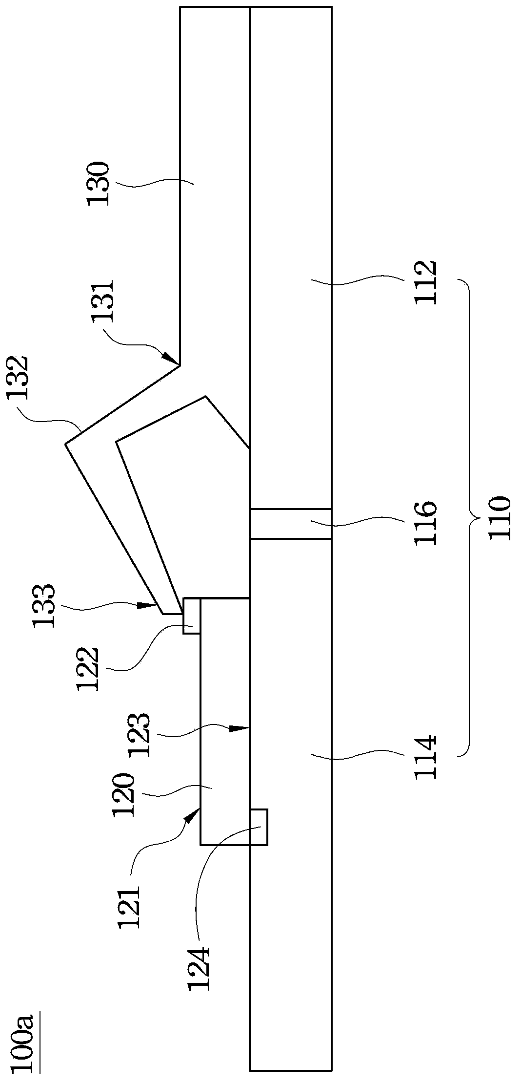
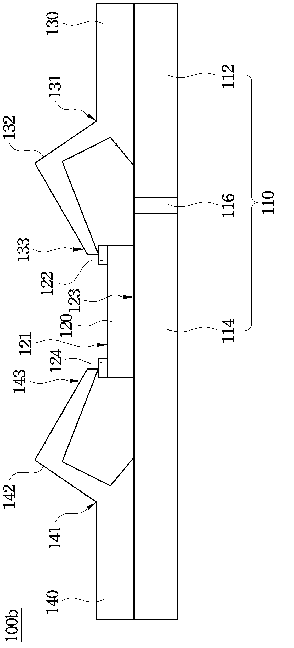
[0061] figure 1 A cross-sectional view of a light emitting diode device 100a according to an embodiment of the present invention is shown. As shown in the figure, the LED device 100 a includes a conductive frame 110 , a LED chip 120 and a first conductive layer 130 . Wherein, the conductive bracket 110 has a first conductive portion 112 , a second conductive portion 114 and an insulating porti...


PUM


Abstract

The invention discloses a light-emitting diode device and a manufacturing method thereof. The light-emitting diode device comprises a conductive support, a light-emitting diode chip and a first conductive layer. The conductive support is provided with a first conductive part, a second conductive part and an insulation part. The insulation part is used for separating the first conductive part and the second conductive part. The light-emitting diode chip is disposed on the second conductive part; and the surface of the light-emitting diode chip is provided with a first electrode and a second electrode. The first conductive layer is formed on the first conductive part and disposed at one side of the light-emitting diode chip. A first edge of the first conductive layer is made into a bendable first conductive extending pin; and one end of the first conductive extending pin is connected with the first electrode of the light-emitting diode chip.

Description

technical field [0001] The invention relates to a light emitting diode device and a manufacturing method thereof. Background technique [0002] Generally speaking, a light emitting diode module includes a light emitting chip, a base and a lens. The lens covers the light-emitting chip, so that the light emitted by the light-emitting chip is relatively uniform. For example, the light emitting chip can be a blue light emitting chip, and the lens can have yellow phosphor. When the blue light passes through the yellow phosphor, the LED module can emit white light. In addition, the light-emitting chip is disposed on the base, and the surface of the light-emitting chip has positive contacts and negative contacts. The surface of the base adjacent to the light-emitting chip has a positive electrode conductive layer and a negative electrode conductive layer. The positive electrode contact and the negative electrode contact of the light-emitting chip need to be connected to the pos...

Claims


Application Information

Patent Timeline
Patent Type & Authority Applications(China)
IPC IPC(8): H01L33/62H01L33/60
CPCH01L24/01H01L2924/12041H01L33/62H01L33/48H01L2933/0066
Inventor 林建志李育群
Owner LEXTAR ELECTRONICS CORP
Why Eureka
Try Eureka