Buffer for raising voltage driving capability
A technology of voltage drive and buffer, applied in the direction of electrical components, logic circuits, pulse technology, etc., can solve problems such as circuit failure, achieve the effect of reducing current, reducing power consumption, and good stability
- Summary
- Abstract
- Description
- Claims
- Application Information
AI Technical Summary
Problems solved by technology
Method used
Image

Examples
Embodiment Construction
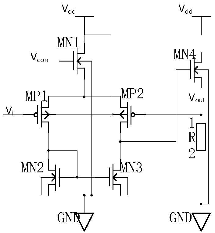
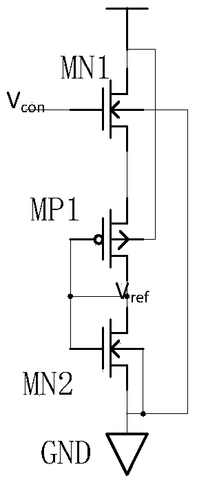
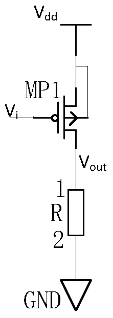
[0013] see figure 1 The high-speed buffer with simple structure, low voltage and high stability of the present invention is composed of four NMOS transistors MN1, MN2, MN3 and MN4, three PMOS transistors MP1, MP2 and MP3, and a resistor R.
[0014] The specific connection relationship is as follows, the drain of the NMOS transistor MN1 and the power supply V dd Connection, the gate is connected to the external control signal V con , the body end is grounded to GND, the source is connected to the source of PMOS transistors MP1 and MP2; the gate of PMOS transistor MP1 is connected to the external input signal V i , body-terminated supply V dd , the drain is connected to the drain and gate of the PMOS transistor MN2 and the gate of the PMOS transistor MN3; the two ends of the resistor R are set to the A terminal and the B terminal, the gate of the PMOS transistor MP2 is connected to the source of the NMOS transistor MN4, and the resistor The A terminal of R is connected, the d...
PUM
 Abstract
Description
Claims
Application Information