Semiconductor device having ohmic recessed electrode
Inactive Publication Date: 2007-06-14
OKI ELECTRIC IND CO LTD
View PDF9 Cites 99 Cited by
Summary
Abstract
Description
Claims
Application Information
AI Technical Summary
This helps you quickly interpret patents by identifying the three key elements:
Problems solved by technology
Method used
Benefits of technology
Benefits of technology
[0017] An object of the present invention is to provide a semiconductor device in which the electric resistance of an ohmic contact formed between a semiconductor film and an ohmic electrode can be reduced sufficiently, and in which variation in the ohmic resistance value caused by manufacturing irregularities is small.
Problems solved by technology
However, when semiconductors having a large energy gap are used, the energy required for alloying is extremely large, and therefore the alloying is difficult.
In a HEMT using a hetero-junction of AlGaN and GaN, alloying is essentially impossible.
However, according to an investigation conducted by the present inventor, the electric resistance of an ohmic contact formed between a semiconductor film and an ohmic electrode cannot be reduced sufficiently with the technique disclosed in K. Kaifu et al.
This technique is also disadvantaged in that variation in the ohmic resistance value caused by manufacturing irregularities is large.
Method used
Image
Click on the blue label to locate the original text in one second.
Reading with bidirectional positioning of images and text.
Examples
first embodiment
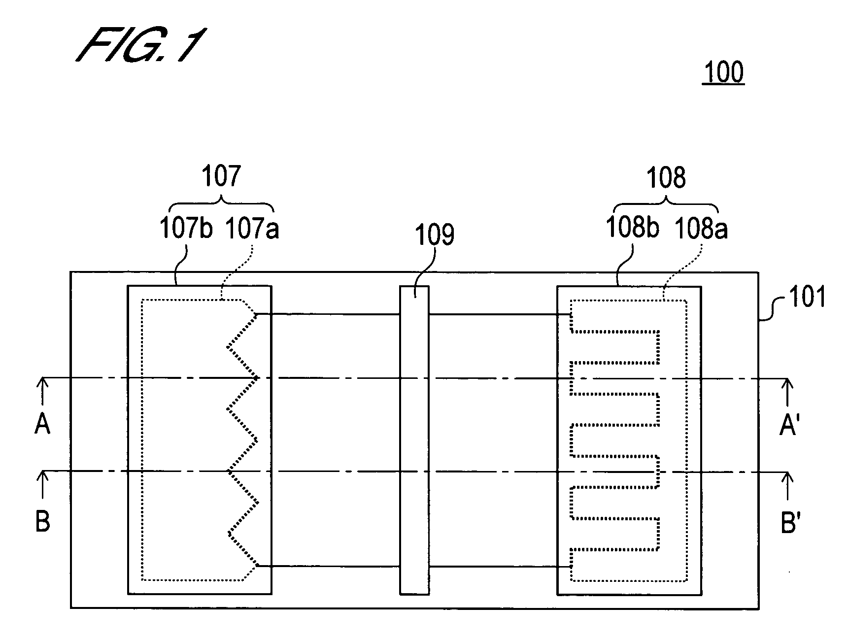
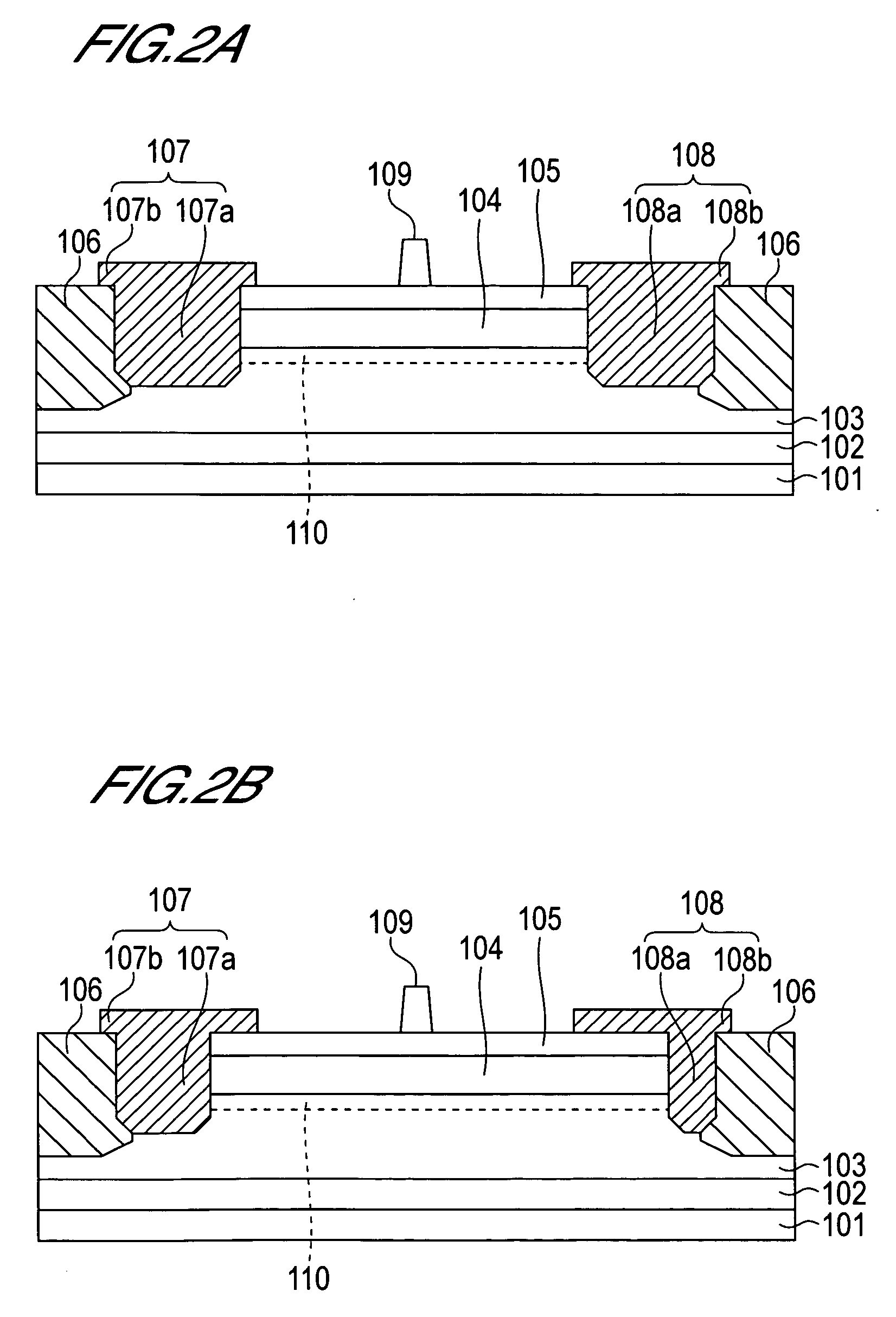
[0035] A semiconductor device according to a first embodiment of the present invention will be described below using an example in which the present invention is applied to a GaN-HEMT, or in other words a HEMT using a GaN layer as a semiconductor layer.
[0036]FIGS. 1, 2A, and 2B show an outline of the structure of the GaN-HEMT according to this embodiment. FIG. 1 is a plan view, FIG. 2A is an A-A′ sectional view of FIG. 1, and FIG. 2B is a B-B′ sectional view of FIG. 1.
[0037] As shown in FIGS. 1, 2A, and 2B, a GaN-HEMT 100 of this embodiment comprises laminated layers, including a buffer layer 102, a channel-forming layer 103, a Schottky layer 104, and a cap layer 105, formed on a semiconductor substrate 101. An isolation region 106, a source electrode 107, a drain electrode 108, and a gate electrode 109 are formed on the laminated layers.
[0038] As the semiconductor substrate 101, a substrate such as an SiC substrate, a sapphire substrate, or a silicon substrate is used, For examp...
second embodiment
[0066] Next, a semiconductor device according to a second embodiment of the present invention will be described using an example in which the present invention is applied to a GaN-HEMT, or in other words a HEMT using a GaN layer as a semiconductor layer.
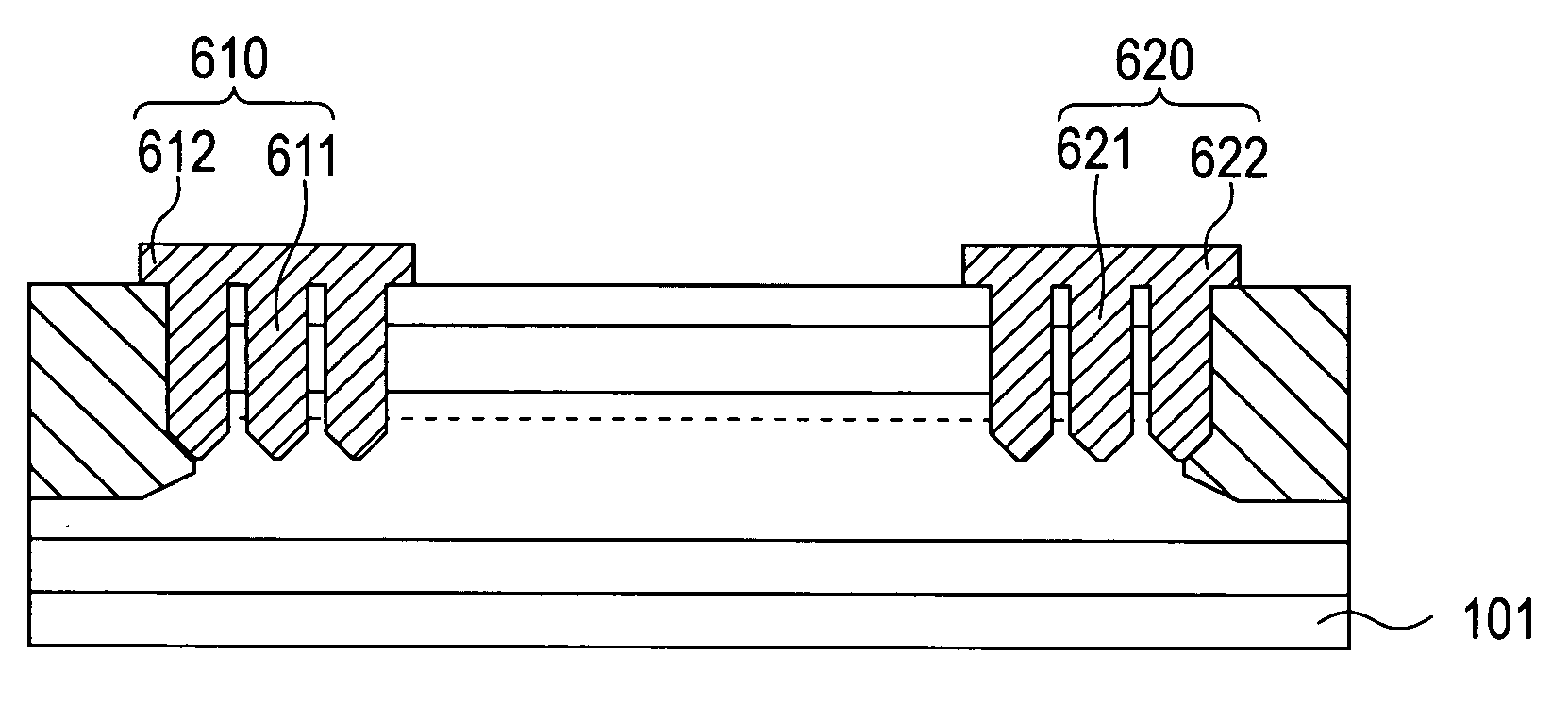
[0067]FIGS. 6 and 7 show an outline of the structure of the GaN-HEMT according to this embodiment. FIG. 6 is a plan view, and FIG. 7 is an E-E′ sectional view of FIG. 6. In FIGS. 6 and 7, constitutional elements having identical reference numerals to those of FIGS. 1 to 2B are identical to the corresponding elements in FIGS. 1 to 2B.
[0068] As is evident from FIGS. 6 and 7, a HEMT 600 according to this embodiment differs from the HEMT 100 according to the first embodiment in the structure of the source electrode and drain electrode.
[0069] A source electrode 610 and a drain electrode 620 are ohmic electrodes. The source electrode 610 comprises a plurality of lower portion electrodes 611 and a single upper portion electrode 612. Simi...
PUM
Abstract
The present invention provides a semiconductor device having a recess-structured ohmic electrode, in which the resistance is small and variation in the resistance value caused by manufacturing irregularities is small. In the semiconductor device of the present invention, a two-dimensional electron gas layer is formed on the interface between a channel-forming layer and a Schottky layer by electrons supplied from the Schottky layer. The ohmic electrode comprises a plurality of side faces in ohmic contact with the two-dimensional electron gas layer. At least a part of side faces of the ohmic electrodes are non-parallel to a channel width direction. In a preferred embodiment of the present invention, the side faces have a saw tooth form or a comb tooth form. Since the contact area between the ohmic electrode and the two-dimensional electron gas layer is increased, ohmic resistance is reduced.
Description
BACKGROUND OF THE INVENTION [0001] 1. Field of the Invention [0002] The present invention relates to a technique for reducing the ohmic resistance of an ohmic electrode having a recessed structure and formed in a semiconductor device. The present invention may be applied to the source electrode and drain electrode of a High Electron Mobility Transistor (HEMT), for example. [0003] 2. Description of Related Art [0004] In the prior art, a HEMT is known as a type of Field EffectTransistor (FET). A feature of a HEMT is that a current path is formed by a two-dimensional electron gas layer generated on the interface between two types of semiconductor film having different band gaps. [0005] Typically, a HEMT comprises a channel-forming layer formed on a substrate and a Schottky layer formed on the channel-forming layer. Films having different band gaps are used as the channel-forming layer and Schottky layer. For example, a GaN film may be used as the channel-forming layer, and an AlGaN fi...
Claims
Application Information
Patent Timeline
Application Date:The date an application was filed.
Publication Date:The date a patent or application was officially published.
First Publication Date:The earliest publication date of a patent with the same application number.
Issue Date:Publication date of the patent grant document.
PCT Entry Date:The Entry date of PCT National Phase.
Estimated Expiry Date:The statutory expiry date of a patent right according to the Patent Law, and it is the longest term of protection that the patent right can achieve without the termination of the patent right due to other reasons(Term extension factor has been taken into account ).
Invalid Date:Actual expiry date is based on effective date or publication date of legal transaction data of invalid patent.

