An array substrate
A technology for arraying substrates and testing signals, applied in nonlinear optics, instruments, optics, etc., can solve the problems of expensive probes and high testing costs, and achieve the effects of reducing testing costs, improving accuracy, and reducing the use of probes
- Summary
- Abstract
- Description
- Claims
- Application Information
AI Technical Summary
Problems solved by technology
Method used
Image


Examples
Embodiment Construction
[0030] In order to make the technical problems, technical solutions and advantages to be solved by the present invention clearer, the following will describe in detail with reference to specific embodiments and accompanying drawings.
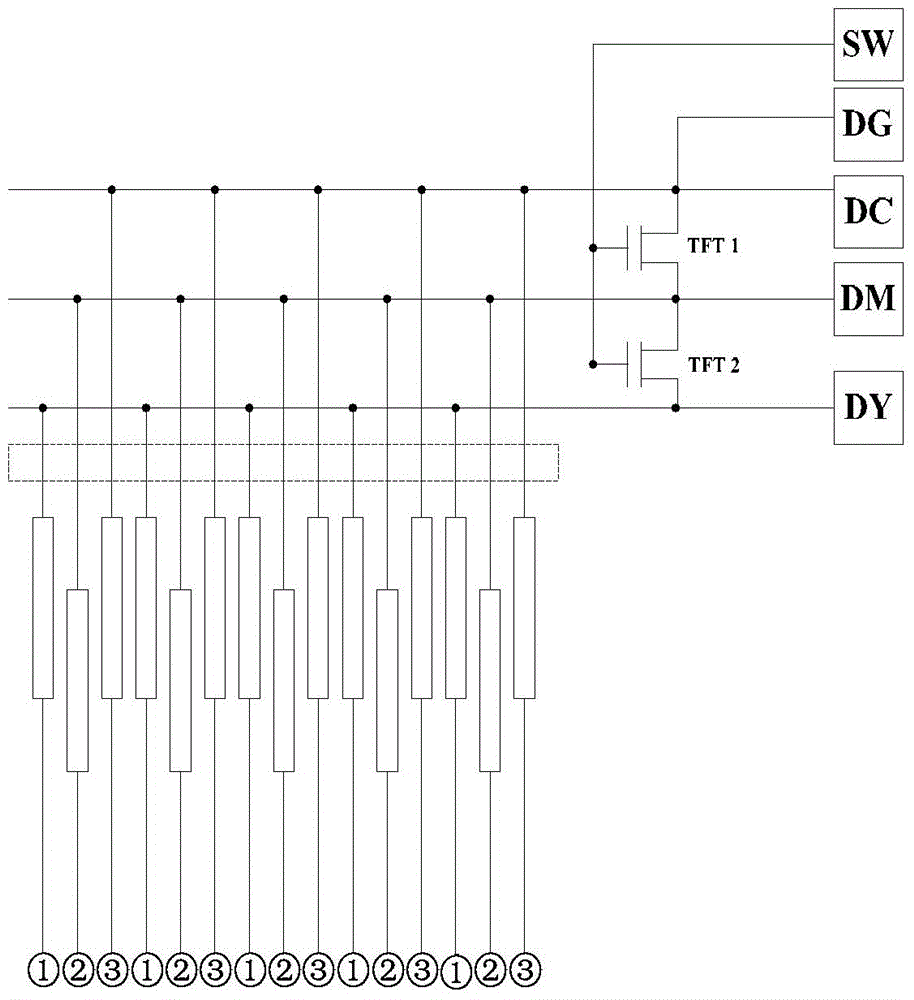
[0031] The embodiment of the present invention solves the problem that when the impurity ions in the panel are quantitatively tested, the test signals in different types of test signal transmission lines are different, resulting in inaccurate detection, and the number of fixture probes used is large. The embodiment of the present invention provides An array substrate, such as figure 1 As shown, wherein the array substrate includes: different types of data lines arranged in the array substrate;
[0032] Corresponding to each type of data line, there is a first test signal input terminal ( figure 1 There are 3 types of data lines, and the corresponding first test signal input terminals are 3, which are DC, DM and DY) test signal transmission li...
PUM
 Abstract
Description
Claims
Application Information
 - R&D
- Intellectual Property
- Life Sciences
- Materials
- Tech Scout
- Unparalleled Data Quality
- Higher Quality Content
- 60% Fewer Hallucinations
Browse by: Latest US Patents, China's latest patents, Technical Efficacy Thesaurus, Application Domain, Technology Topic, Popular Technical Reports.
© 2025 PatSnap. All rights reserved.Legal|Privacy policy|Modern Slavery Act Transparency Statement|Sitemap|About US| Contact US: help@patsnap.com