Supercharge Your Innovation With Domain-Expert AI Agents!

AMOLED array basal plate and display device

An array substrate and array technology, applied in the field of AMOLED array substrates and display devices, can solve problems such as poor adhesion, easy erosion by water and oxygen, and influence of organic light-emitting materials

Active Publication Date: 2014-04-02
BOE TECH GRP CO LTD
View PDF4 Cites 31 Cited by
  • Summary
  • Abstract
  • Description
  • Claims
  • Application Information

AI Technical Summary

Problems solved by technology

Wherein, the cathode lead 160 is made of a metal material, used to connect the cathode 180 to an external signal, and is usually located in a non-display area (that is, a non-A-A area) on the array substrate. Due to poor adhesion between the metal and the pixel definition layer 170, the display The layer between the cathode lead 160 and the pixel definition layer 170 at the edge of the panel is easily corroded by water and oxygen, and the corrosion of water and oxygen inside will affect the organic light-emitting materials.

Method used


Image

  • AMOLED array basal plate and display device
  • AMOLED array basal plate and display device
  • AMOLED array basal plate and display device

Examples


Embodiment Construction

[0027] The specific implementation manners of the present invention will be further described in detail below in conjunction with the accompanying drawings and embodiments. The following examples are used to illustrate the present invention, but are not intended to limit the scope of the present invention.

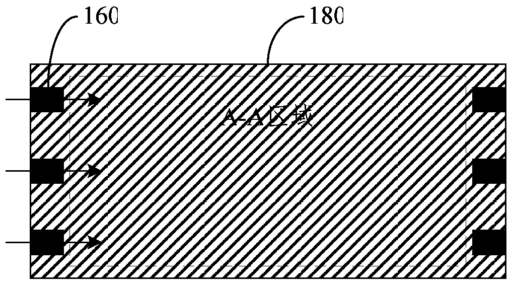
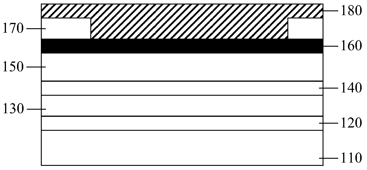
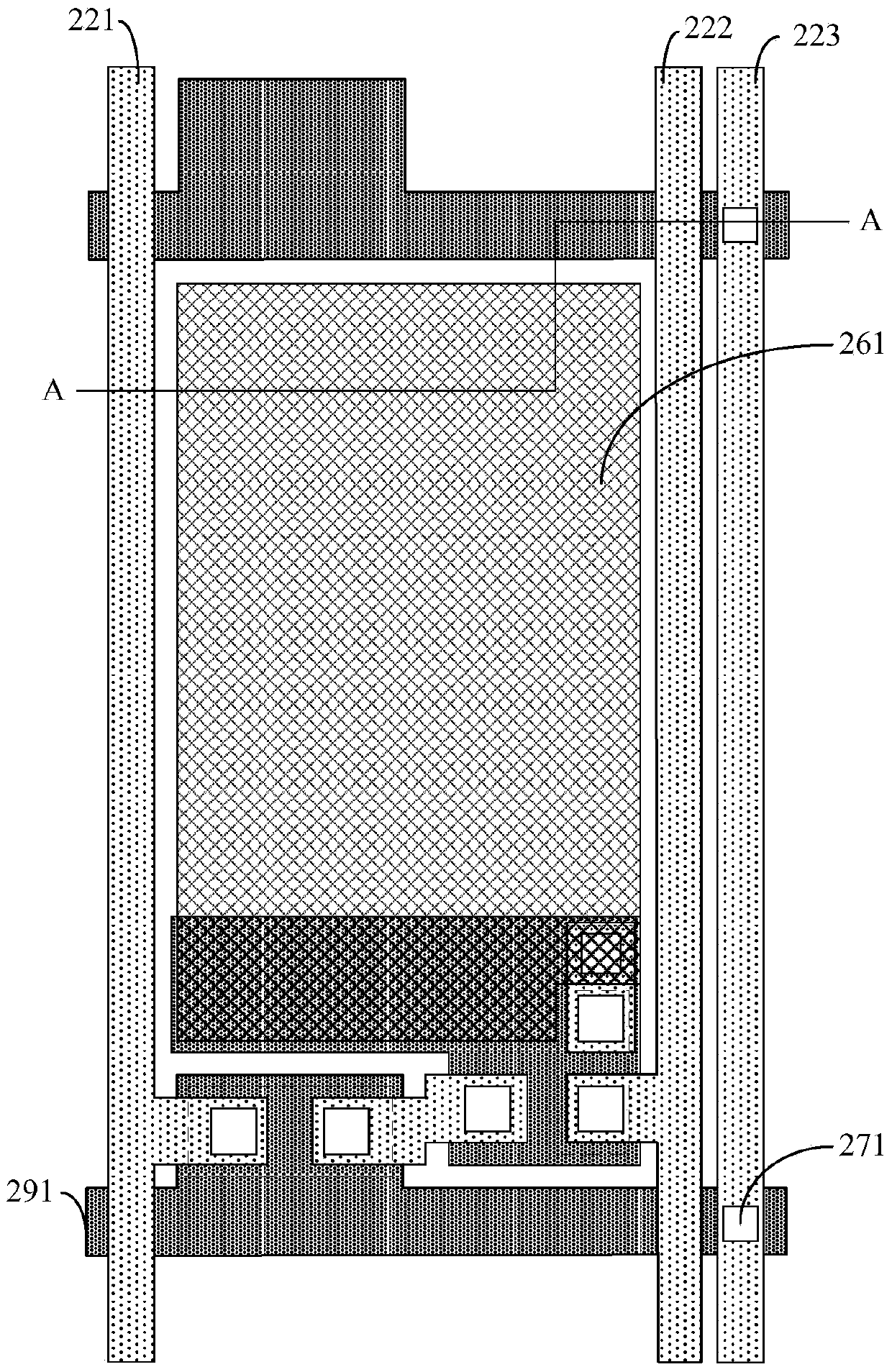
[0028] Such as Figure 2a and 2b As shown, the AMOLED array substrate of the present invention includes several pixel structures formed in an array on the base substrate 210 . Each pixel structure is surrounded by a gate line 291 and a signal line 221 and a power supply 222 perpendicular to the gate line 291 . Each pixel structure includes: a thin film transistor structure, an anode 261 , a cathode 280 , and an organic light emitting layer 300 between the anode 261 and the cathode 280 . The specific hierarchy is as Figure 2a and 2b As shown, it includes from bottom to top: base substrate 210, gate metal layer (including: gate line 291, gate of thin film transistor), ...


PUM


Abstract

The invention discloses an AMOLED array basal plate. The AMOLED array basal plate comprises a plurality of pixel structures formed on a substrate basal plate in an array mode; each pixel structure is formed by encircling a grid line and a signal line and a power supply line which are vertical to the grid line; each pixel structure comprises a thin film transistor structure, an anode, a cathode and an organic lighting layer between the anode and the cathode; each anode is positioned at the area corresponding to each pixel structure; each cathode is a transparent electrode covering the whole array basal plate; the AMOLED array basal plate also comprises first cathode auxiliary lines parallel with the signal lines; each first cathode auxiliary line penetrates through at least two dot-shaped via holes to be connected with the corresponding cathode; at least one end of each first cathode auxiliary line extends to the edge of the array basal plate for connecting each cathode with an external cathode signal circuit. The cathodes are connected to the edge of the array basal plate by the first cathode auxiliary lines, and water-oxygen corrosion caused by the contact between a metal layer, at the edge, of a cathode lead with a pixel definition layer is avoided.

Description

technical field [0001] The invention relates to the field of display technology, in particular to an AMOLED array substrate and a display device. Background technique [0002] For a top-emitting AMOLED display device, the cathode is formed by a transparent electrode (such as: ITO), and it is a block electrode that covers the array substrate as a whole. Such as Figure 1a and 1b As shown, the array substrate structure includes from bottom to top: a base substrate 110 , a gate metal layer 120 , a gate insulating layer 130 , a source-drain electrode layer 140 , a passivation layer 150 , a cathode lead 160 , a pixel definition layer 170 and a cathode 180 . Wherein, the cathode lead 160 is made of a metal material, used to connect the cathode 180 to an external signal, and is usually located in a non-display area (that is, a non-A-A area) on the array substrate. Due to poor adhesion between the metal and the pixel definition layer 170, the display The layer between the cathode ...

Claims


Application Information

Patent Timeline
IPC IPC(8): H01L27/32H01L51/52
Inventor 永山和由
Owner BOE TECH GRP CO LTD
Features
  • R&D
  • Intellectual Property
  • Life Sciences
  • Materials
  • Tech Scout
  • Unparalleled Data Quality
  • Higher Quality Content
  • 60% Fewer Hallucinations
Learn More