Supercharge Your Innovation With Domain-Expert AI Agents!

Array substrate, display panel and display device

A technology of array substrates and substrate substrates, which is applied in semiconductor devices, electrical components, circuits, etc., can solve problems such as poor corrosion of static reduction layers, achieve the effect of improving yield and reliability, and reducing the risk of failure

Active Publication Date: 2021-03-23
BOE TECH GRP CO LTD +1
View PDF9 Cites 0 Cited by
  • Summary
  • Abstract
  • Description
  • Claims
  • Application Information

AI Technical Summary

Problems solved by technology

[0005] The object of the present invention is to overcome the deficiency that the electrostatic reduction layer in the prior art is prone to poor corrosion, and to provide an array substrate, a display panel with the array substrate installed, and a display panel with the static reduction layer. display device

Method used


Image

  • Array substrate, display panel and display device
  • Array substrate, display panel and display device
  • Array substrate, display panel and display device

Examples


Embodiment Construction

[0043] Example embodiments will now be described more fully with reference to the accompanying drawings. Example embodiments may, however, be embodied in many forms and should not be construed as limited to the embodiments set forth herein; rather, these embodiments are provided so that this disclosure will be thorough and complete, and will fully convey the concept of example embodiments to those skilled in the art. The same reference numerals in the drawings denote the same or similar structures, and thus their detailed descriptions will be omitted.

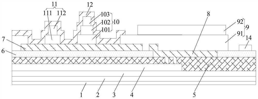
[0044] refer to figure 1 A schematic structural diagram of an array substrate in the related art is shown, the array substrate includes a base substrate 1, a buffer layer 2 is disposed on the base substrate 1, and a first gate insulating layer 3 is disposed on the buffer layer 2, A first conductor layer 4 is provided on the first gate insulating layer 3, a second gate insulating layer 5 is provided on the first gate insulatin...


PUM


Abstract

The invention relates to the technical field of display, and provides an array substrate, a display panel and a display device. The array substrate comprises a substrate, an electrostatic reduction layer, an organic material layer group and a water blocking layer, wherein the electrostatic reduction layer is arranged on the substrate; the organic material layer group is arranged on the surface, deviating from the substrate, of the electrostatic reduction layer; the water blocking layer is arranged on the surface, deviating from the substrate, of the organic material layer group, the organic material layer group is wrapped by the water blocking layer, a groove is formed in the water blocking layer, and the extending direction of the groove is consistent with the extending direction of a separation line of the peripheral area and the display area. The organic material layer group is wrapped by the water blocking layer, so that water oxygen corrosion to the electrostatic reduction layer due to the fact that water oxygen reaches the electrostatic reduction layer through the organic material layer group is effectively avoided, and the yield and reliability of the OLED product are improved. The groove can effectively prevent the water blocking layer from being spread to a display area by cracks generated by external collision, so that the risk of packaging failure of an OLED productis reduced.

Description

technical field [0001] The present invention relates to the field of display technology, in particular to an array substrate, a display panel installed with the array substrate, and a display device installed with the display panel. Background technique [0002] During the manufacturing process of OLED products, reliability testing of OLED products is required. At present, during the reliability test of OLED products, it is easy to have poor corrosion caused by the erosion and oxidation of the static electricity reduction layer by water and oxygen, thereby reducing the yield and reliability of OLED products. [0003] Therefore, it is necessary to study a new array substrate, a display panel equipped with the array substrate, and a display device equipped with the display panel. [0004] The above information disclosed in this Background section is only for enhancement of understanding of the background of the invention and therefore it may contain information that does not ...

Claims


Application Information

Patent Timeline
Patent Type & Authority Patents(China)
IPC IPC(8): H01L27/32H01L51/52
Inventor 周桢力蒋志亮刘伟
Owner BOE TECH GRP CO LTD
Features
  • R&D
  • Intellectual Property
  • Life Sciences
  • Materials
  • Tech Scout
  • Unparalleled Data Quality
  • Higher Quality Content
  • 60% Fewer Hallucinations
Learn More