Novel laminated perovskite photoelectric component and preparation method thereof
A technology of photoelectric components and perovskite, which is applied in the field of new laminated perovskite photoelectric components and its preparation, can solve the problems of perovskite being eroded by water and oxygen, the area of photoactive area becomes smaller, and perovskite degradation. Achieve the effects of easy large-scale production, avoid water and oxygen erosion, and improve stability
- Summary
- Abstract
- Description
- Claims
- Application Information
AI Technical Summary
Problems solved by technology
Method used
Image

Examples
preparation example Construction
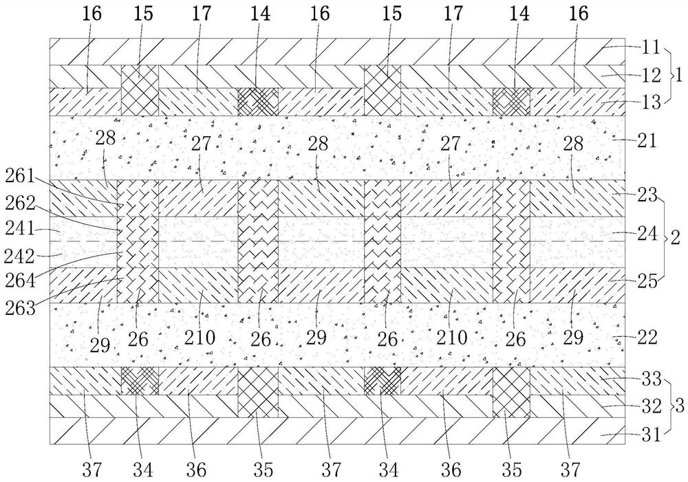
[0055] The present invention also discloses a method for preparing the aforementioned novel stacked perovskite optoelectronic component, comprising the following steps:
[0056] First prepare the upper half device 1 and the lower half device 3 respectively, then prepare the first perovskite layer 21 and the second perovskite layer 22 on the upper half device 1 and the lower half device 3 respectively, and then prepare the surface of the first perovskite layer 21 Prepare the middle first composite transport layer 23 and the upper first middle spacer layer 261, prepare the middle second composite transport layer 25 and the lower first middle spacer layer 263 on the surface of the second perovskite layer 22, and then prepare the middle first composite transport layer on the surface of the second perovskite layer 22. The upper composite electrode 241 and the upper second intermediate partition layer 262 are prepared on the surface of 23, the lower composite electrode 242 and the lo...
Embodiment 1
[0088] The method for preparing the first novel laminated perovskite optoelectronic component of the present invention includes the following steps:
[0089] Step 11. The FTO conductive glass substrate is cleaned and treated with ultraviolet and ozone for 30 minutes.
[0090] Step 12: Using a mask, alternately deposit electron transport material titanium dioxide, isolation material silicon oxide, and hole transport material poly-TPD on the surface of the FTO to obtain an upper electron transport layer 16, an upper isolation layer 14 and an upper hole transport layer 17, wherein , an upper blank section for preparing the upper blocking layer 15 is reserved between a part of the upper electron transport layer 16 and the upper hole transport layer 17 .
[0091]Step 13 , using a laser etching method to remove the upper conductive electrode 12 of the upper blank section to expose the upper substrate 11 . The etching width is 1 μm to 1 mm. Then, using a mask, the upper blank secti...
Embodiment 2
[0099] The preparation method of the second novel stacked perovskite photoelectric component of the present invention includes the following steps:
[0100] Step 21 to Step 25: The same as Step 11 to Step 15 respectively.
[0101] Step 26 : Repeat steps 21 to 23 to obtain the lower half device 3 . The lower half device 3 was placed flat and preheated to 70°C. The prepared perovskite precursor solution with a concentration of 0.6 mol / L is deposited on the substrate, the solutes are cesium iodide, lead iodide and dimethylamine hydroiodide, the molar ratio is 1:1:1, and the solvent is N,N-Dimethylformamide. Then, the isopropanol solution of methylamine hydrochloride with a concentration of 60 mmol / ml was sprayed onto the surface of the perovskite precursor film, annealed at 210 °C for 10 min, and washed with isopropanol to remove excess methylamine hydrogen after cooling. Chlorate, resulting in 150 nm thick CsPbI 3 The perovskite layer is the lower perovskite layer 22 .
[0...
PUM
| Property | Measurement | Unit |
|---|---|---|
| thickness | aaaaa | aaaaa |
| thickness | aaaaa | aaaaa |
| width | aaaaa | aaaaa |
Abstract
Description
Claims
Application Information
 - R&D
- Intellectual Property
- Life Sciences
- Materials
- Tech Scout
- Unparalleled Data Quality
- Higher Quality Content
- 60% Fewer Hallucinations
Browse by: Latest US Patents, China's latest patents, Technical Efficacy Thesaurus, Application Domain, Technology Topic, Popular Technical Reports.
© 2025 PatSnap. All rights reserved.Legal|Privacy policy|Modern Slavery Act Transparency Statement|Sitemap|About US| Contact US: help@patsnap.com