Novel perovskite photoelectric component and preparation method thereof
A technology of photoelectric components and perovskite, which is applied in the field of new perovskite photoelectric components and its preparation, can solve the problems of perovskite being eroded by water and oxygen, the area of photoactive area becomes smaller, and the degradation of perovskite, so as to achieve easy Large-scale production, avoiding water and oxygen erosion, and improving stability
- Summary
- Abstract
- Description
- Claims
- Application Information
AI Technical Summary
Problems solved by technology
Method used
Image

Examples
preparation example Construction
[0050] The present invention also discloses a method for preparing the aforementioned novel perovskite optoelectronic component, comprising the following steps:
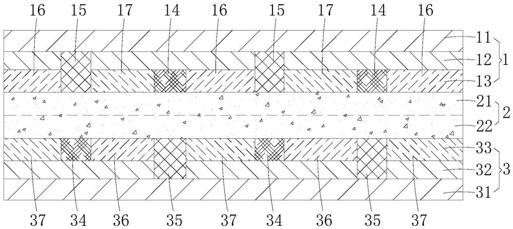
[0051] First prepare the upper half device 1 and the lower half device 3 respectively, and then prepare the upper half perovskite layer 21 and the lower half perovskite layer on the upper composite transport layer 13 of the upper half device 1 and the lower composite transport layer 33 of the lower half device 3, respectively The ore layer 22, and finally the upper half device 1 and the lower half device 3, which have been prepared with the upper half perovskite layer 21 and the lower half perovskite layer 22, are stacked face to face with each other, wherein the upper perovskite layer 21 and the lower calcium The titanium ore layer 22 is laminated and fused with each other to form a complete perovskite layer 2, and the upper electron transport layer 16, the upper hole transport layer 17, the upper isolation layer 14 ...
Embodiment 1
[0077] The preparation method of the first novel perovskite optoelectronic component of the present invention comprises the following steps:
[0078] Step 11. The ITO conductive glass substrate was cleaned and treated with ultraviolet ozone for 30 minutes.
[0079] Step 12. Using a mask, alternately deposit electron transport material tin oxide, isolation material aluminum oxide, hole transport material nickel oxide on the ITO surface to obtain the upper electron transport layer 16, the upper isolation layer 14 and the upper hole transport layer 17, wherein , an upper blank section for preparing the upper blocking layer 15 is reserved between the upper electron transport layer 16 and the upper hole transport layer 17 .
[0080] Step 13. Use laser etching to remove the upper conductive electrode 12 of the upper blank section to expose the upper substrate 11 . The etching width is 1 μm to 1 mm. Then, the isolation material polyamide is filled to form the upper isolation layer ...
Embodiment 2
[0086] The preparation method of the second novel perovskite optoelectronic component of the present invention comprises the following steps:
[0087] Step 21. The ITO conductive glass substrate was cleaned and treated with ultraviolet ozone for 30 minutes. Using a mask, the electron transport material titanium dioxide and the hole transport material copper phthalocyanide are alternately deposited on the surface of the ITO to obtain the upper electron transport layer 16 and the upper hole transport layer 17 respectively.
[0088] Step 22. Use the laser etching method to remove the upper conductive electrode 12 at the bottom of the upper blank groove where the upper isolation layer 15 is located, exposing the upper substrate 11 at the bottom, and the etching width is 1 micrometer to 1 mm.
[0089] Step 23. Using the mask, deposit the material polyamide for preparing the upper isolation layer and the upper isolation layer in the reserved upper blank groove respectively to prepar...
PUM
| Property | Measurement | Unit |
|---|---|---|
| width | aaaaa | aaaaa |
| width | aaaaa | aaaaa |
Abstract
Description
Claims
Application Information
 - R&D
- Intellectual Property
- Life Sciences
- Materials
- Tech Scout
- Unparalleled Data Quality
- Higher Quality Content
- 60% Fewer Hallucinations
Browse by: Latest US Patents, China's latest patents, Technical Efficacy Thesaurus, Application Domain, Technology Topic, Popular Technical Reports.
© 2025 PatSnap. All rights reserved.Legal|Privacy policy|Modern Slavery Act Transparency Statement|Sitemap|About US| Contact US: help@patsnap.com