Semiconductor device, apparatus of estimating lifetime, method of estimating lifetime

A semiconductor and life-span technology, applied in semiconductor devices, semiconductor/solid-state device components, measuring devices, etc., can solve the problem that it is difficult to specify the location of raised cracks in advance

Inactive Publication Date: 2014-04-09
KK TOSHIBA
View PDF7 Cites 0 Cited by
  • Summary
  • Abstract
  • Description
  • Claims
  • Application Information

AI Technical Summary

Problems solved by technology

[0006] However, since the nature of the stress mainly occurring in the bump and the area receiving the stress look different depending on the rigidity of the circuit board or the packaging conditions of the semiconductor device, it is difficult to specify in advance where a crack occurs in the bump at an early stage

Method used


Image

  • Semiconductor device, apparatus of estimating lifetime, method of estimating lifetime
  • Semiconductor device, apparatus of estimating lifetime, method of estimating lifetime
  • Semiconductor device, apparatus of estimating lifetime, method of estimating lifetime

Examples


no. 1 example )

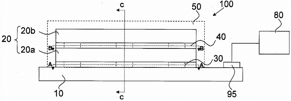
[0023] figure 1 is a diagram illustrating the semiconductor device 100 of the first embodiment.

[0024] The semiconductor device 100 is configured to include a stacked semiconductor chip 20 formed by stacking a plurality of semiconductor chips in a stacking direction (upward in the figure) on a circuit board 10 such as an interposer. The stacked semiconductor chips 20 are configured to include a plurality of first semiconductor chips 20a including a lowermost semiconductor chip and a plurality of second semiconductor chips 20b stacked over the first semiconductor chips 20a.

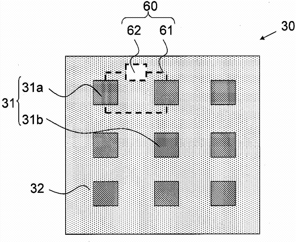
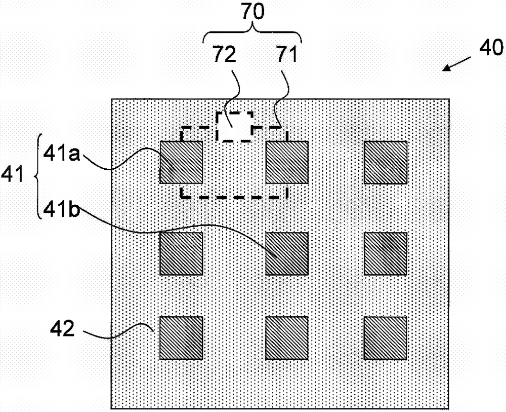
[0025] The circuit board 10 and the first semiconductor chips 20 a are interconnected by the first interconnection unit 30 , and two of the first semiconductor chips 20 a are interconnected by the first interconnection unit 30 . The first semiconductor chip 20 a and the second semiconductor chip 20 b are interconnected by the second interconnection unit 40 , and two of the second semiconductor chips 20 ...

no. 2 example )

[0053] Figure 5 is a diagram illustrating a semiconductor device 200 of the second embodiment. Denote with the same reference numerals as the figure 1 The components of the semiconductor device 100 are the same, and the detailed description will not be repeated. In the semiconductor device 200 , the first signal from the first detection unit 62 and the second signal from the second detection unit 72 are used to estimate the load state in the semiconductor device 200 and to estimate the lifetime of the semiconductor device 200 .

[0054] Apart from figure 1 In addition to the semiconductor device 100 , the semiconductor device 200 further includes a storage unit 210 , a load estimating unit 220 , and a lifetime estimating unit 230 . As the storage unit 210, a storage device 400 such as a memory is used. As the load estimating unit 220 and the lifetime estimating unit 230 , an arithmetic processing unit 500 such as a CPU is used. The load estimation unit 220 is electricall...


PUM


Abstract

The invention relates to a semiconductor device, an apparatus of estimating a lifetime, method of estimating a lifetime. According to one embodiment, a semiconductor device includes a circuit board, a plurality of semiconductor chips stacked above the circuit board, first and second bumps, third and fourth bumps, and first and second detection units. The first and second bumps are provided in either a gap between the circuit board and the semiconductor chip or a gap between the two semiconductor chips. The third and fourth bumps are provided in any of gaps other than the gap in which the first and second bumps are provided. The first detection unit is electrically connected to the first bump to detect damage of the first bump and to generate a first signal indicating the damage of the first bump. The second detection unit is electrically connected to the third bump to detect damage of the third bump and to generate a second signal indicating the damage of the third bump.

Description

[0001] Cross References to Related Applications [0002] This application is based upon and claims the benefit of priority from a prior Japanese Patent Application Serial No. 2012-218786 filed on September 28, 2012, the entire contents of which are incorporated herein by reference. technical field [0003] Embodiments described herein generally relate to semiconductor devices, apparatus for estimating lifetime, and methods for estimating lifetime. Background technique [0004] In a stacked semiconductor device (hereinafter referred to as a semiconductor device), two or more semiconductor chips are stacked over a circuit board. The circuit board and the lowest chip are interconnected by bumps. The lowermost semiconductor chip and the semiconductor chips stacked above the lowermost chip are interconnected by bumps. When a semiconductor device is used for a long period of time, cracks are usually generated in the bumps. [0005] The generation of cracks in the bumps leads to...

Claims


Application Information

Patent Timeline
Patent Type & Authority Applications(China)
IPC IPC(8): H01L23/498H01L23/544H01L25/16
CPCG01R31/318513H01L2224/16145G01R31/31924
Inventor 山寄优广畑贤治
Owner KK TOSHIBA
Why Eureka
Try Eureka