A circuit board optical automatic detection device

An optical automatic detection and detection device technology, which is applied to measuring devices, material analysis through optical means, scientific instruments, etc., can solve problems such as poor image shooting quality, misjudgment of appearance inspection equipment, vibration of mobile devices, etc. Management, damage avoidance and cost saving effects

Inactive Publication Date: 2016-08-17
惠州元创自动化科技有限公司
View PDF3 Cites 0 Cited by
  • Summary
  • Abstract
  • Description
  • Claims
  • Application Information

AI Technical Summary

Problems solved by technology

[0004] Those skilled in the art have tried to improve the efficiency of detection by increasing the speed of the X-Y moving device, but in the actual implementation process, it is found that when the moving speed is too fast, the moving device will vibrate, resulting in poor image quality and causing appearance inspection equipment Misjudgment

Method used


Image

  • A circuit board optical automatic detection device
  • A circuit board optical automatic detection device

Examples


Embodiment Construction

[0024] The present invention will be further described in detail below with reference to the embodiments and the accompanying drawings, but the embodiments of the present invention are not limited thereto.

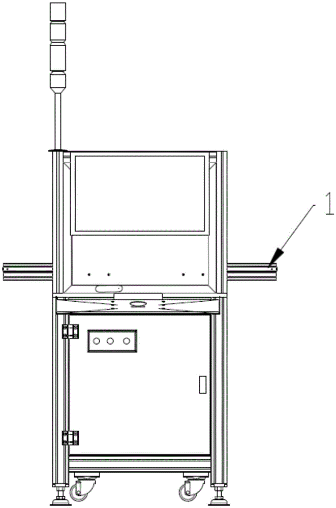
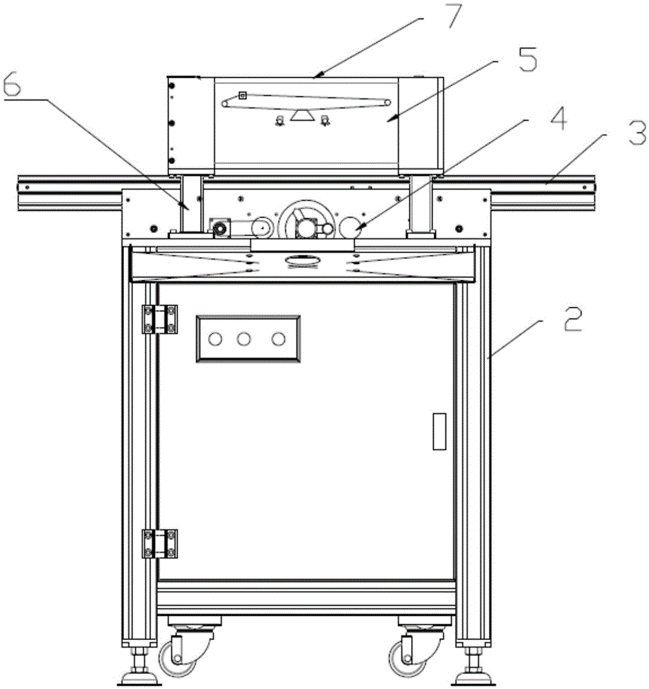
[0025] Such as figure 1 and figure 2 As shown, a circuit board optical automatic detection device includes a feeding device, a detection device and a computer equipped with image analysis software.

[0026] in:

[0027] The feeding device includes a feeding transmission guide rail 1 and a thickness detection sensor. The thickness detection sensor is located under the feeding transmission guide rail 1. The thickness detection sensor transmits detection data to the computer through wireless communication.

[0028] The detection device includes a base 2 , a detection transmission guide rail 3 erected on the base 2 , a pressing and positioning mechanism 4 for fixing the product on the detection transmission guide rail 3 , and a scanner 5 arranged above the detection transmi...


PUM


Abstract

The invention discloses an optical automatic detection device of a circuit board. The optical automatic detection device comprises a material inlet device, a detecting device and a computer with image analysis software, wherein the detecting device comprises a base, a detecting transmission guide rail arranged on the base, a compressing positioning mechanism for fixing a product on the detecting transmission guide rail and a scanner arranged above the detecting transmission guide rail. The optical automatic detection device provided by the invention has the advantages that the scanning detection mode is adopted to replace the detection mode of multi-time photograph, and the detection efficiency is improved; a condition that an image joint is easy to distort so as to cause a detection error is avoided, a condition that the service life of a shaft is damaged and the image-taking quality is poor is avoided, the circuit board to be detected is not damaged because of the vibration, the scanner is common and is easy to purchase, and the cost of the optical automatic detection device is low compared with the traditional movable type camera device.

Description

technical field [0001] The invention relates to the technical field of circuit board appearance detection, in particular to a circuit board optical automatic detection device. Background technique [0002] As the core components of electronic products, circuit boards play an extremely important role. Therefore, stricter requirements are put forward for the quality of circuit boards. Among them, in order to ensure that there are no breaks or short circuits on the surface of the circuit board, as well as no leakage or wrong installation of plug-ins, and whether the stickers and solder paste are biased or missing, an appearance inspection will be carried out after the board is pasted and plug-ins. [0003] In the prior art, the working principle of the appearance inspection equipment is: use the X-Y moving device to drive the camera to move, the camera moves to the corresponding position of the circuit board under test for sampling, and then uses the computer to compare and ana...

Claims


Application Information

Patent Timeline
Patent Type & Authority Patents(China)
IPC IPC(8): G01N21/956
Inventor 邹小波
Owner 惠州元创自动化科技有限公司
Why Eureka
Try Eureka