Power-on/power-down output tri-state control circuit for CMOS device power supply
A technology of three-state control and control circuit, which is applied in the direction of electrical components, electronic switches, pulse technology, etc., and can solve problems such as interface device damage, bus error reversal, etc.
- Summary
- Abstract
- Description
- Claims
- Application Information
AI Technical Summary
Problems solved by technology
Method used
Image
Examples
Embodiment Construction
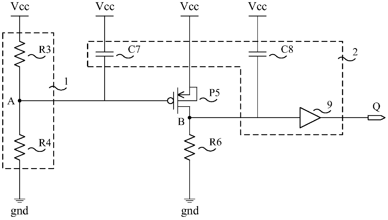
[0016] Such as figure 1 Shown is a structural diagram of a CMOS device power supply power on and off output tri-state control circuit of the present invention, including a MOS tube series resistance voltage divider circuit 1, a PMOS switch tube P5 and a shaping filter circuit 2. The MOS transistor series resistance voltage divider circuit 1 includes a resistor R3 and a resistor R4 , and the shaping filter circuit 2 includes a capacitor C7 , a capacitor C8 and an output buffer 9 .
[0017] The MOS tubes used in the present invention are all enhanced MOS tubes.
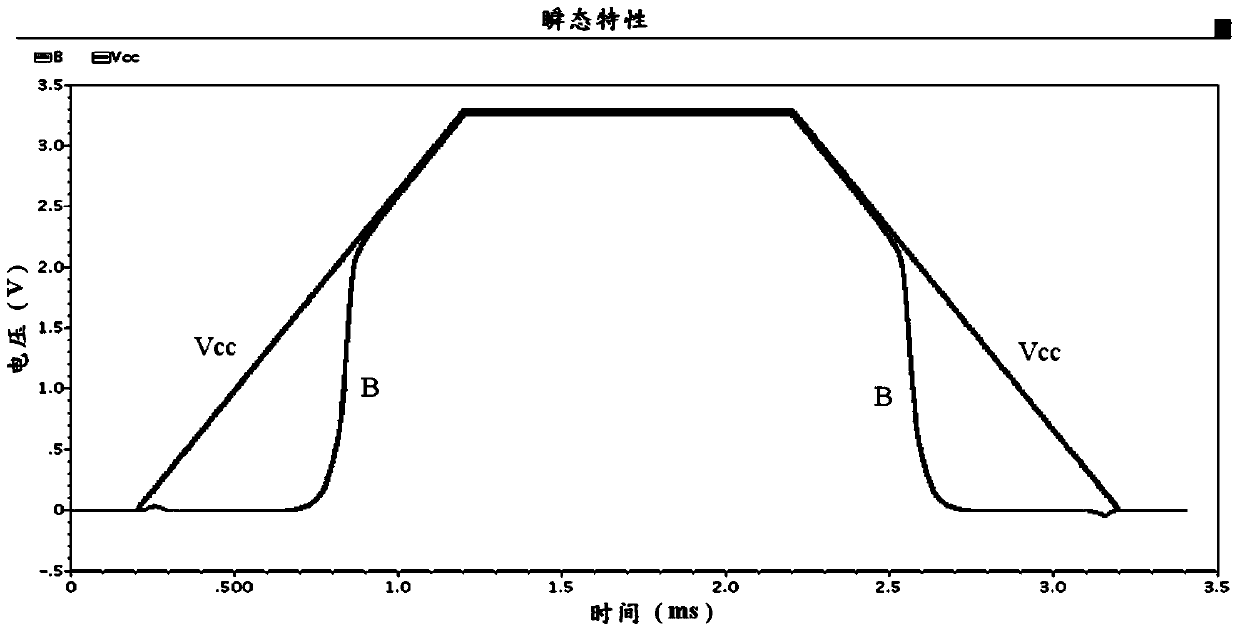
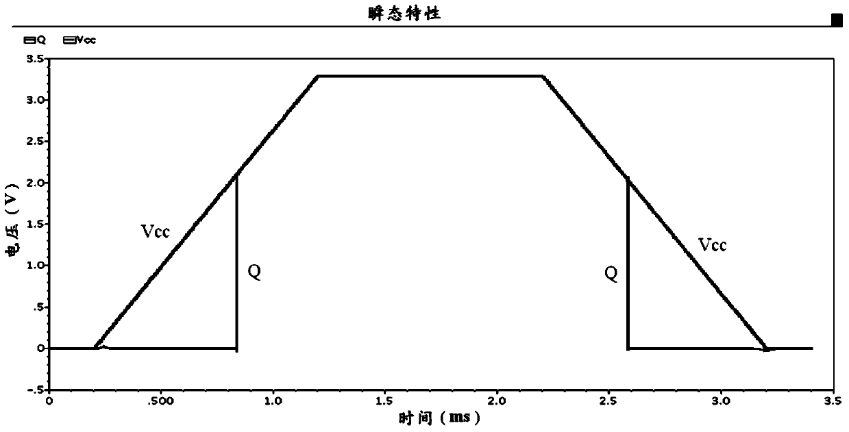
[0018] During the power-on or power-off process of the device, the MOS transistor series resistance voltage divider circuit 1 obtains the proportional voltage divider value of the power supply voltage Vcc at node A through the voltage divider of the resistor R3 and the resistor R4, and connects it to the PMOS switch tube P5 The gate terminal controls the turn-on and turn-off of the PMOS switch P5. When the voltage dif...
PUM
 Abstract
Description
Claims
Application Information


