Chip-on-film module, display panel and display

A display panel and chip-on-chip technology, applied in the field of chip-on-chip COF modules, display panel CELL and display, can solve the problem of long panel wiring and achieve the effect of eliminating color shift

Active Publication Date: 2014-04-30
SHENZHEN CHINA STAR OPTOELECTRONICS TECH CO LTD
View PDF4 Cites 10 Cited by
  • Summary
  • Abstract
  • Description
  • Claims
  • Application Information

AI Technical Summary

Problems solved by technology

[0003] However, especially in single-source COF products, due to the limitations of the fan-out (Fan-out) design on the LCD panel Cell, the traces on both sides of the panel are longer than the middle, such as figure 1 shown

Method used


Image

  • Chip-on-film module, display panel and display
  • Chip-on-film module, display panel and display
  • Chip-on-film module, display panel and display

Examples


Embodiment Construction

[0026] The implementation of the present invention will be described in detail below in conjunction with the accompanying drawings and examples, so as to fully understand and implement the process of how to apply technical means to solve technical problems and achieve technical effects in the present invention. It should be noted that, as long as there is no conflict, each embodiment and each feature in each embodiment of the present invention can be combined with each other, and the formed technical solutions are all within the protection scope of the present invention.

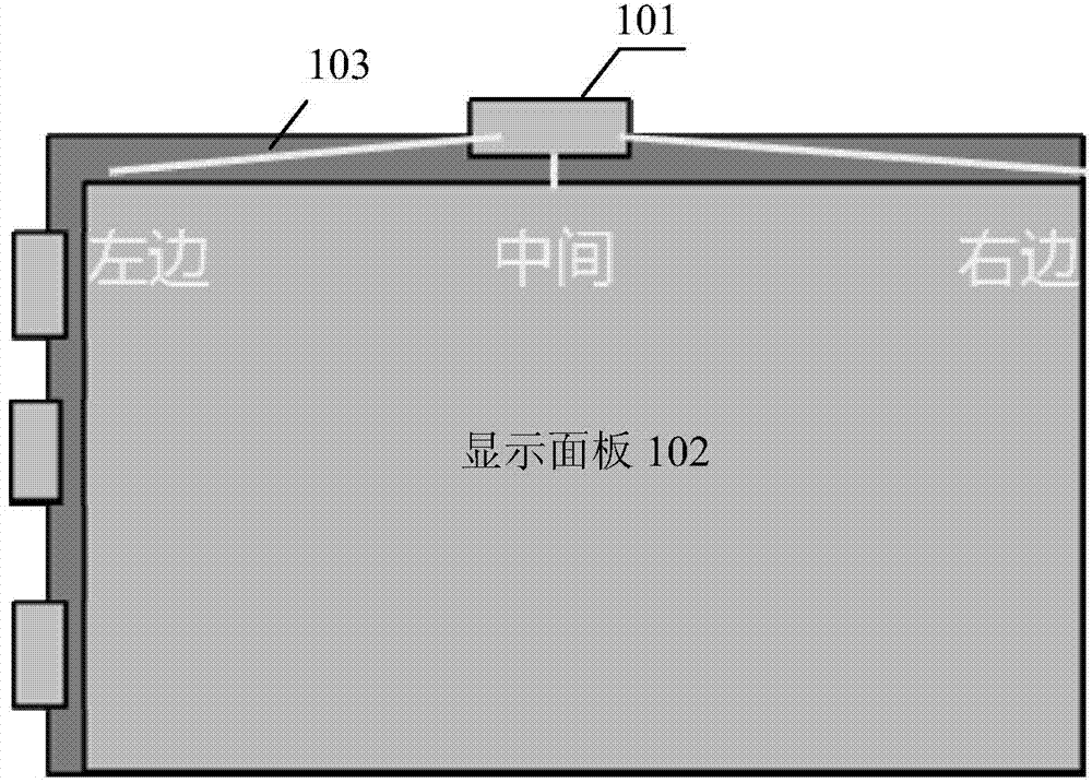
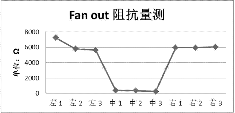
[0027] Figure 4 A schematic diagram of the composition structure of the display is shown. It includes a driving circuit board 104 , a COF display module 101 , and a Cell display panel 102 . In the Cell process stage, the COF display module 101 is connected to the fan-out Fan-out terminal of the Cell display panel 102 through the metal bonding area 105 of its output terminal (such as a golden finger structu...


PUM


Abstract

The invention discloses a chip-on-film module. The COF module comprises a flexible substrate, a chip and a first set of terminals, wherein the chip is arranged on the flexible substrate, and the first set of terminals are arranged on the flexible substrate and electrically connected with the output end of the chip. All the terminals of the first set of terminals comprise metal bonding areas which are used for making contact with fan-out terminals of a display panel and have different areas, so that equivalent resistances on all fan-out circuits are the same or similar. The invention further provides the display panel. The display panel comprises a display unit and a set of fan-out terminals, wherein a plurality of pixel arrays are arranged on the display unit, the set of fan-out terminals are connected with the display unit, and all the terminals in the fan-out terminals comprise metal bonding areas which are used for making contact with the first set of terminals of the COF display module and have different areas, so that the equivalent resistances on all the fan-out circuits are the same or similar. According to the COF module and the display panel, the display color cast problem caused by resistance nonuniformity on the fan-out circuits on the Cell display panle can be eliminated.

Description

technical field [0001] The invention relates to the field of display technology, in particular to a chip-on-film COF module, a display panel CELL and a display. Background technique [0002] The popularization of mobile electronic products and large-screen displays has promoted the rapid development of low-cost, high-density and mass-scale electronic production technologies. Large-sized electronic products such as LCD monitors, LCD TVs, and plasma TVs, and small and medium-sized electronic products such as mobile phones and digital cameras are all developing in light, thin, and small sizes. This requires new products with high density, small volume, and free installation. A generation of packaging technology to meet the above needs. COF (Chip On Flex, or Chip On Film, flip chip) packaging technology came into being. This technology is a chip soft film construction technology that fixes the chip on the flexible circuit board. It uses a flexible circuit board as a packaged ...

Claims


Application Information

Patent Timeline
Patent Type & Authority Applications(China)
IPC IPC(8): H01L23/498G02F1/1362
CPCG02F1/13452H01L23/49838H01L23/4985H01L2924/0002
Inventor 李厚斌
Owner SHENZHEN CHINA STAR OPTOELECTRONICS TECH CO LTD
Why Eureka
Try Eureka