Method for processing anode device of ultraviolet photon counting integral imaging detector

An imaging detector and ultraviolet photon technology, which is applied in the manufacture of electrode assemblies, electrical components, cold cathodes, etc., can solve the problems of difficulty in achieving the accuracy of cross-position sensitive anodes, and inability to finely process upper conductive layers and insulating layers, etc. Achieve the effect of overcoming low machining accuracy, avoiding crosstalk between electrodes and reducing anode size

Active Publication Date: 2014-05-07
东莞市中科原子精密制造科技有限公司
View PDF3 Cites 3 Cited by
  • Summary
  • Abstract
  • Description
  • Claims
  • Application Information

AI Technical Summary

Problems solved by technology

[0005] The present invention proposes a new processing method for the anode device of the ultraviolet photon counting integral imaging detector, in order to overcome the difficulty in achieving the accuracy of the cross position-sensitive anode in the traditional mechanical processing technology, and the inability of the general photolithography technology to finely process the upper conductive layer and the Technical Difficulty of Insulation Layer

Method used


Image

  • Method for processing anode device of ultraviolet photon counting integral imaging detector
  • Method for processing anode device of ultraviolet photon counting integral imaging detector
  • Method for processing anode device of ultraviolet photon counting integral imaging detector

Examples


Embodiment Construction

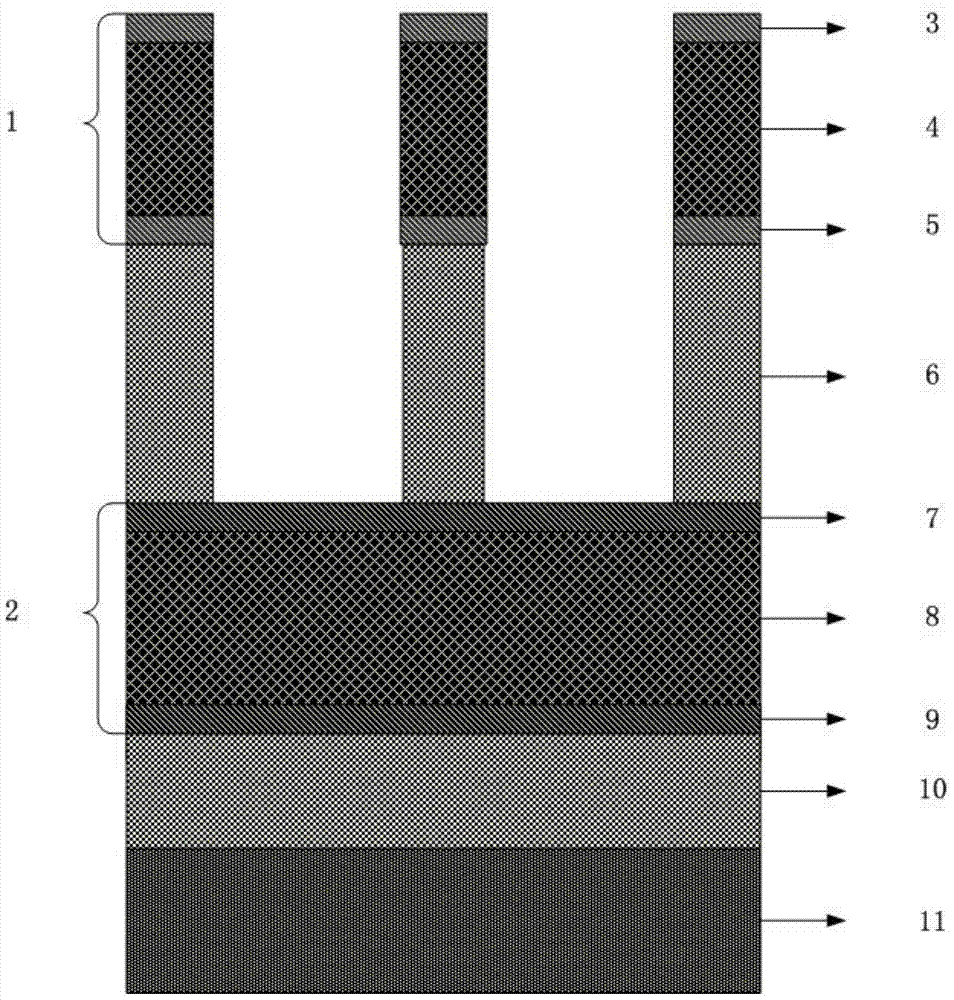
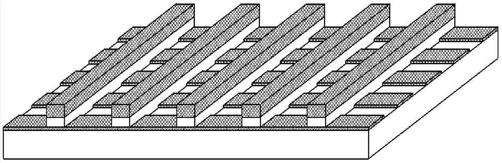
[0032] The present invention uses the widely commercialized PCB technology and relatively mature photolithography technology, combined with the unique design of the cross-position sensitive anode, processes the double-sided copper-clad PCB board, and processes the cross-position-sensitive anode that meets the precision requirements. . Such as figure 1 , figure 2 As shown, the specific process steps are as follows:

[0033] Step 1: Prefabrication of a photolithography mask. The parameters of the photolithography mask plate: the length is 100mm, the width is 100mm, and the period of the rectangular stripes is 0.5mm. The stripe width is 0.4mm, the stripe spacing is 0.1mm, and there is a rectangular groove between two adjacent rectangular stripes.

[0034] Step 2: Etching the anode pattern. Select two identical PCB boards, the characteristics of the PCB board: the upper and lower surfaces are covered by copper layer, the copper layer thickness is 4-10μm; the middle is a flat...


PUM


Abstract

The invention provides a method for processing an anode device of an ultraviolet photon counting integral imaging detector so as to overcome technical problems that the precision of a crossed position-sensitive anode is difficult to achieve by adopting traditional machining technologies, and that an upper conductive layer and an insulating layer cannot be precisely processed by adopting general photoetching technologies. The PCB (printed circuit board) processing technology adopted by the method mainly comprises the steps of precasting a photoetching diaphragm plate, etching an anode pattern, bonding modules, precisely covering the photoetching diaphragm plate, cutting an insulating material by adopting femtosecond laser and connecting a via plated though hole interface. The method provided by the invention is high in processing precision, simple in process, high in yield, low in cost, and capable of carrying out mass production in a large scale.

Description

technical field [0001] The invention belongs to the technical field of multi-anode processing, and in particular relates to a processing method for a position-sensitive anode suitable for a microchannel anode detector. Background technique [0002] The anode device to be processed and manufactured in the present invention is a cross-position-sensitive anode, which is divided into upper and lower layers. Both the upper layer and the lower layer include a plurality of rectangular conductive strips with the same size. Parallel, the rectangular conductive strips of the lower layer are parallel to each other in the same plane, and a straight line insulation channel is formed between the adjacent rectangular conductive strips of the same layer; all the rectangular conductive strips of the upper layer and the lower layer form a cross grid as a whole, and each rectangular conductive strip is independent Output charge signal. [0003] Compared with the traditional position-sensitive...

Claims


Application Information

Patent Timeline
Patent Type & Authority Applications(China)
IPC IPC(8): H01J9/02H01J9/18
Inventor 朱香平邓国宝
Owner 东莞市中科原子精密制造科技有限公司
Why Eureka
Try Eureka