Glue control method of step package substrate

A technology for packaging substrates and steps, which is applied in the manufacturing of electrical components, electrical solid-state devices, semiconductor/solid-state devices, etc., can solve the problems of infeasibility, narrow application range, uncontrollable glue flow, etc., to ensure effective size and ensure glue flow. residual effect

Active Publication Date: 2014-05-07
JIANGNAN INST OF COMPUTING TECH
View PDF2 Cites 5 Cited by
  • Summary
  • Abstract
  • Description
  • Claims
  • Application Information

AI Technical Summary

Problems solved by technology

In fact, it is difficult to avoid the partial flow of glue from the gap between the filler and the conductor to pollute the pad if the conventional filler resisting glue is selected, such as Figure 4 shown
[0006] On the other hand, for prepregs with a small amount of glue flow, the amount of glue flow is less than 0.5mm. By reasonably designing the window size of the prepreg, the glue flow on the groove conductor can be kept within the control range (the glue flow does not exceed 20% of the area of ​​the conductor area) , but for the lamination of multi-layer boards, in order to ensure that the glue flow between layers fills the conductor gap and ensure reliability, a prepreg with a large amount of glue flow is generally selected to better fill the pattern gap, which leads to glue flow. Uncontrollable
Therefore, the scope of application of using a small amount of prepreg to open windows to control glue flow is very narrow, and most stacked structures are not feasible.

Method used


Image

  • Glue control method of step package substrate
  • Glue control method of step package substrate
  • Glue control method of step package substrate

Examples


Embodiment Construction

[0028] In order to make the content of the present invention clearer and easier to understand, the content of the present invention will be described in detail below in conjunction with specific embodiments and accompanying drawings.

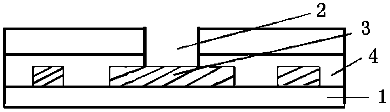
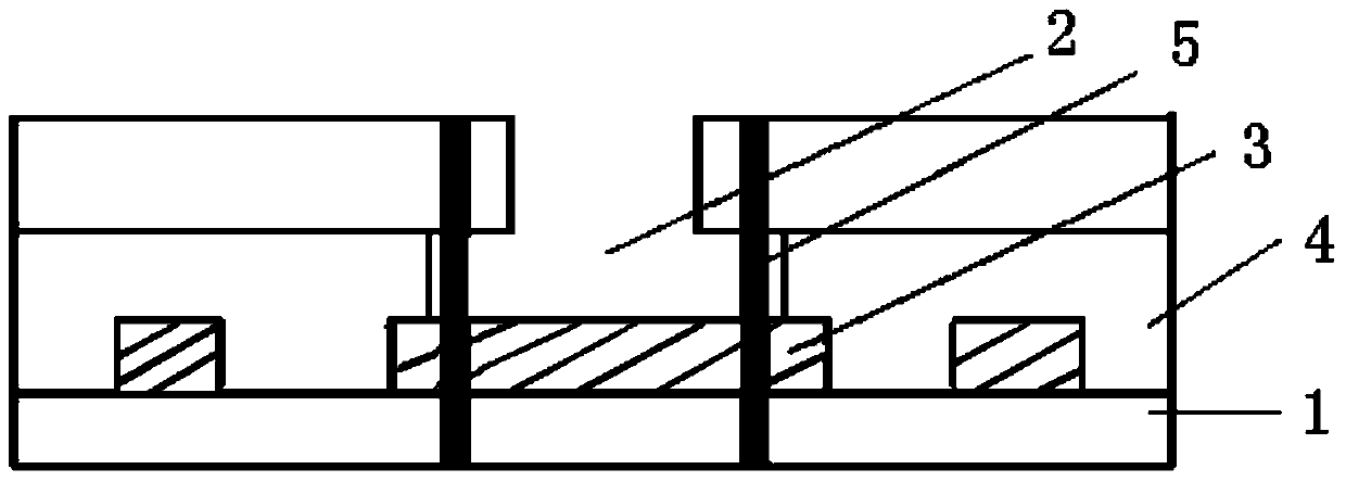
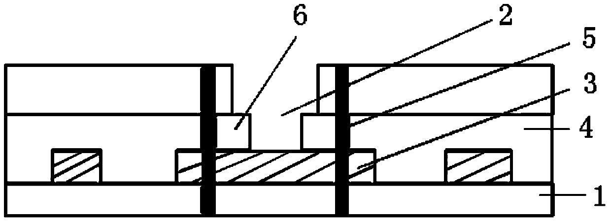
[0029] The present invention solves some limitations of the glue control by the two methods of the prior art mentioned in the background technology, and proposes a new glue control method, which prevents glue by silk-screening a layer of peelable glue on the conductor exposed at the groove. The glue ensures that there is no glue residue in the conductor at the groove position, which ensures the subsequent wiring or welding of the groove conductor.

[0030] Specifically, Figure 5 A flow chart of a method for controlling glue on a stepped packaging substrate according to a preferred embodiment of the present invention is schematically shown.

[0031] Such as Figure 5 As shown, the step packaging substrate glue control method according to the p...


PUM


Abstract

The invention provides a glue control method of a step package substrate. The glue control method comprises the following steps that firstly, acid washing is conducted on an inner single chip of a package structure with a groove, and the groove is provided with a layer of peelable glue in a silk printing mode; secondly, the structure provided with the peelable glue in the silk printing mode is baked, so that the peelable glue is solidified and shaped; thirdly, after the peelable glue is solidified and shaped, brown oxidation is conducted on the inner single chip, and lamination is conducted on the inner single chip so as to form a multilayer board; fourthly, before a finished product is milled, the peelable glue is removed, so that a conductor under the peelable glue is exposed. The glue control method of the step package substrate can effectively prevent the situation that flow glue remains on the exposed conductor in the groove.

Description

technical field [0001] The invention relates to the field of integrated circuit manufacturing, and more specifically, the invention relates to a method for controlling glue on a stepped packaging substrate. Background technique [0002] When designing some packaging substrates, the chip or soldering position on the substrate medium 1 is made into a step shape (or groove 2), such as figure 1 As shown, the conductor is exposed at this place (conductor 3 exposed at the groove), and it is used for wiring or soldering devices after surface treatment (gold plating or tin spraying). This part of the exposed conductor needs to be wired or welded later, so the conductor must be kept intact and completely exposed, that is, no dielectric residue is allowed on the conductor, so glue control is required. [0003] During conventional lamination, the prepreg 4 is windowed in the exposed area of ​​the conductor. Due to the difference in pattern distribution and different heating, the glue...

Claims


Application Information

Patent Timeline
Patent Type & Authority Applications(China)
IPC IPC(8): H01L21/56
CPCH01L23/00H01L21/486H01L21/4867H01L23/498H01L23/49827H01L2924/0002H01L2924/00H01L21/561
Inventor 刘秋华穆敦发吴小龙吴梅珠徐杰栋胡广群梁少文
Owner JIANGNAN INST OF COMPUTING TECH
Why Eureka
Try Eureka