Piezoelectric electret film button
A piezoelectric electret and film technology, applied in the field of piezoelectric electret film keys, can solve the problems of increased process cost, complex structure, low sensitivity, etc., and achieve the effects of saving power consumption, small size and long service life
- Summary
- Abstract
- Description
- Claims
- Application Information
AI Technical Summary
Problems solved by technology
Method used
Image
Examples
Embodiment 1
[0033] Example 1: Combining figure 1 , the piezoelectric electret film button, including a piezoelectric electret film 1, an upper surface electrode 2 attached to the upper surface of the piezoelectric electret film 1, and a lower surface electrode attached to the lower surface of the piezoelectric electret film 1 3. The upper surface encapsulation layer 4 and the lower surface encapsulation layer 5 encapsulated in the outer layer of the upper surface electrode 2 and the lower surface electrode 3, the surface layer 6 located on the upper surface encapsulation layer, and the lower surface shield located below the lower surface encapsulation layer 5 Layer 7 and base layer 8.
[0034] The piezoelectric electret film 1 is an organic film containing a micro-hole structure, and permanent charges are stored inside the micro-hole structure.
[0035] The lower surface electrode 3, such as figure 2 As shown, it consists of three mutually independent conductive electrodes 31 , and eac...
Embodiment 2
[0041] Embodiment 2: another kind of embodiment of the present invention, overall lamellar structure is identical with embodiment 1, and difference is:
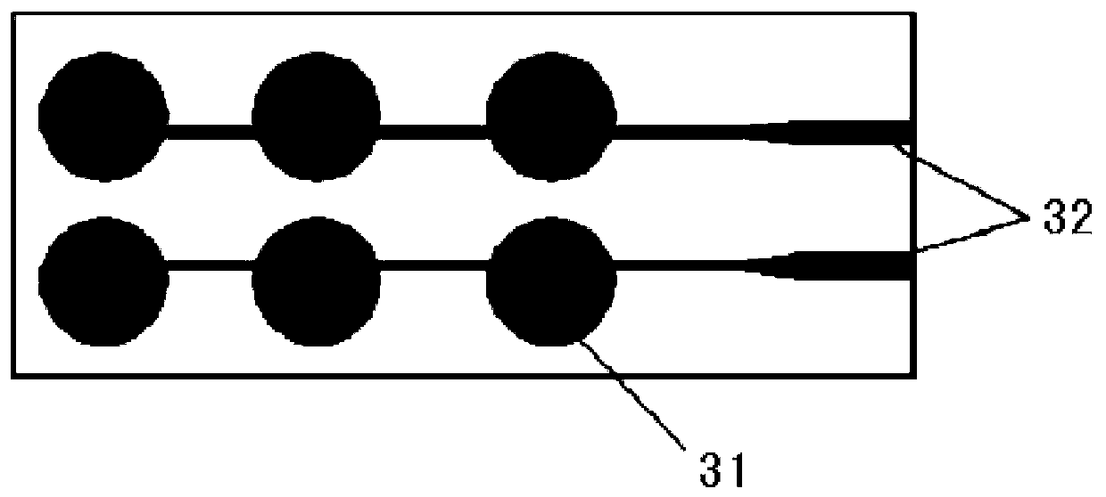
[0042] The lower surface electrode 3, such as image 3 As shown, it consists of two vertically arranged conductive electrode groups, and each conductive electrode group is composed of three horizontally arranged conductive electrodes 31 in series, and each conductive electrode group is led out by a wire 32 respectively.
[0043] The upper surface electrode 2, such as Figure 5 As shown, it consists of three sets of conductive electrode groups arranged horizontally, and each conductive electrode group is formed by two vertically arranged conductive electrodes 21 in series, and each conductive electrode group is led out by a wire 22 respectively.
Embodiment 3
[0044] Embodiment 3: Another embodiment of the present invention is based on Embodiment 1 or Embodiment 2, modifying the structure of the upper surface electrode 2 to be composed of a whole piece of conductive electrode 21, which is led out by a wire 22, and The coverage area of the upper surface electrode 2 ≥ the coverage area of the lower surface electrode 3, such as Image 6 shown.
PUM
 Abstract
Description
Claims
Application Information


