Liquid crystal display panel packaging structure

A liquid crystal panel and packaging structure technology, applied in the field of liquid crystal panel packaging structure, can solve the problems of broken COF, unable to set retaining wall structure, fragments, etc., and achieve the effect of avoiding damage

Active Publication Date: 2014-05-14
TCL CHINA STAR OPTOELECTRONICS TECH CO LTD
View PDF10 Cites 11 Cited by
  • Summary
  • Abstract
  • Description
  • Claims
  • Application Information

AI Technical Summary

Problems solved by technology

[0002] refer to figure 1 As shown, the existing small-sized OLED panel adopts thinner material as the base material, and the planar compression resistance of the panel is relatively weak. At the same time, in order to achieve a better picture display effect, the PCB of the small-sized OLED panel The COF at the end is usually designed wider, and the distance from the COF to the edge of the panel is very small. Such a structure makes it impossible to install a retaining wall structure on the COF side of the panel. The LCD panel is not easy to fix in the packing box. Risk of Broken COF

Method used


Image

  • Liquid crystal display panel packaging structure
  • Liquid crystal display panel packaging structure
  • Liquid crystal display panel packaging structure

Examples


Embodiment Construction

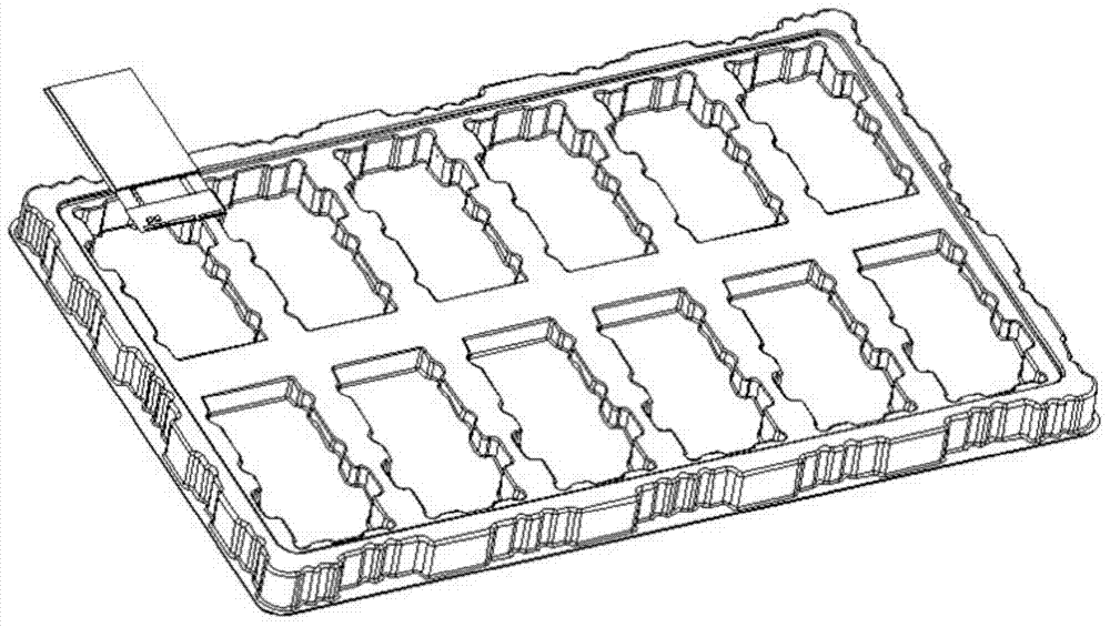
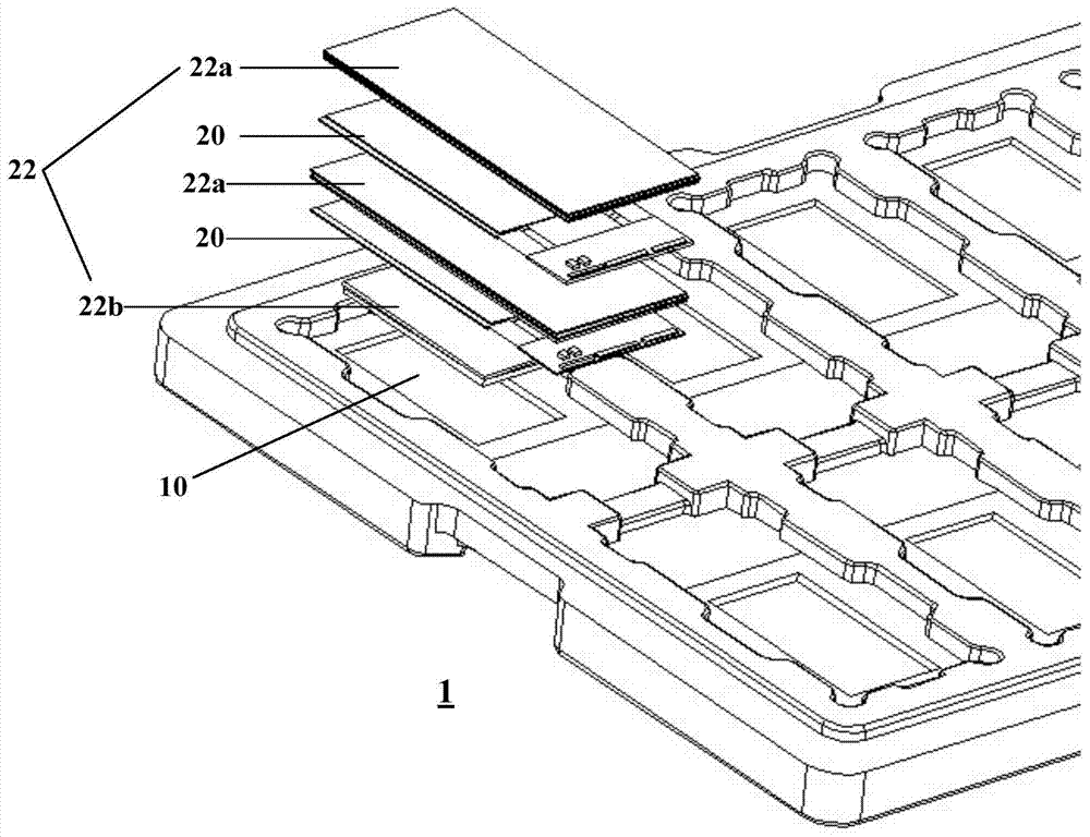
[0015] During the transportation of the liquid crystal panel, in order to protect the liquid crystal panel from shaking left and right to hit the packaging structure and cause damage to the liquid crystal panel, a packaging structure that can prevent the liquid crystal panel from shaking during transportation is provided. Reference figure 2 with image 3 As shown, a liquid crystal panel packaging structure of the present invention is used for packaging liquid crystal panels during transportation. The packaging structure 1 is provided with a plurality of storage slots 10, and the liquid crystal panels 20 are respectively stored in the packaging structure 1, wherein The packaging structure 1 further includes spacers 22 arranged on the upper and lower sides of the liquid crystal panel 20 and attracting each other to prevent the liquid crystal panel 20 from shaking and hitting the side surface of the receiving slot 10 during transportation.

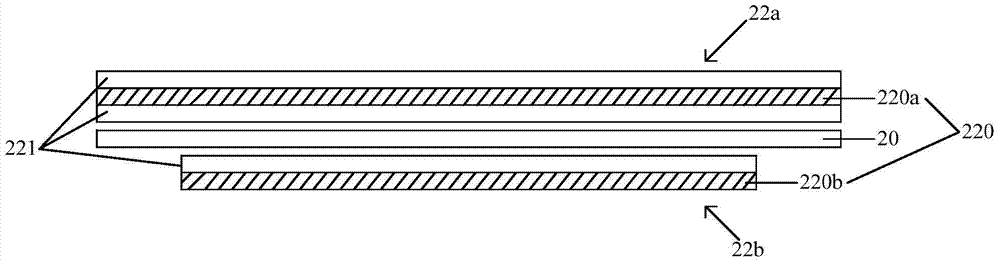
[0016] Among them, refer to figure 2 As...


PUM


Abstract

The invention provides a liquid crystal display panel packaging structure which is used for packaging liquid crystal display panels in the process of transportation. The liquid crystal display panel packaging structure is provided with a plurality of containing grooves. The liquid crystal display panels are respectively contained in the packaging structure. The packaging structure further comprises pads which are arranged on the upper side and the lower side of each liquid crystal display panel and attract each other so that each liquid crystal display panel is prevented from shaking and impacting the side faces of the corresponding containing groove in the process of transportation. The upper pads and the lower pads are additionally arranged, so that the liquid crystal display panels are clamped tightly; each liquid crystal display panel is attracted and attached to the portion between blocked layers through the mutual attraction of magnetic pieces internally arranged between the upper pads and the lower pads, so that the liquid crystal display panels are prevented from shaking vertically in the process of transportation; meanwhile, the blocked layers which are high in friction coefficient and resistant to static electricity adhere to the liquid crystal display panels, so that generated friction is large and the liquid crystal display panels are prevented from shaking laterally.

Description

Technical field [0001] The invention relates to a packaging structure, in particular to a liquid crystal panel packaging structure. Background technique [0002] Reference figure 1 As shown, the existing small-size OLED panel uses a thinner material as the base material, and the plane pressure resistance of the panel is relatively weak. At the same time, in order to achieve a better screen display effect, the PCB of the small-size OLED panel The COF at the end is usually designed to be wider, and the distance from the COF to the edge of the panel is very small. This structure makes the COF side of the panel unable to install a retaining wall structure. The LCD panel is not easy to fix in the packaging box. The risk of breaking the COF. Summary of the invention [0003] Based on the shortcomings of the prior art, the main purpose of the present invention is to provide a liquid crystal panel packaging structure that can prevent the liquid crystal panel from shaking in the vertical ...

Claims


Application Information

Patent Timeline
Patent Type & Authority Applications(China)
IPC IPC(8): B65D81/05B65D85/30
CPCB65D81/022B65D81/113B65D81/127B65D2313/04B65D85/48B65D81/3813
Inventor 岳亮陈仕祥萧宇均
Owner TCL CHINA STAR OPTOELECTRONICS TECH CO LTD
Why Eureka
Try Eureka