NAND Flash memorizer and implementing method and system of NAND Flash memorizer

A technology of memory and storage block, which is applied in the field of data storage and can solve the problems of low unit price and large capacity of 1 bit

Active Publication Date: 2014-05-21
GIGADEVICE SEMICON (BEIJING) INC
View PDF5 Cites 2 Cited by
  • Summary
  • Abstract
  • Description
  • Claims
  • Application Information

AI Technical Summary

Problems solved by technology

But the capacity is large, and the

Method used


Image

  • NAND Flash memorizer and implementing method and system of NAND Flash memorizer
  • NAND Flash memorizer and implementing method and system of NAND Flash memorizer
  • NAND Flash memorizer and implementing method and system of NAND Flash memorizer

Examples


Embodiment 1

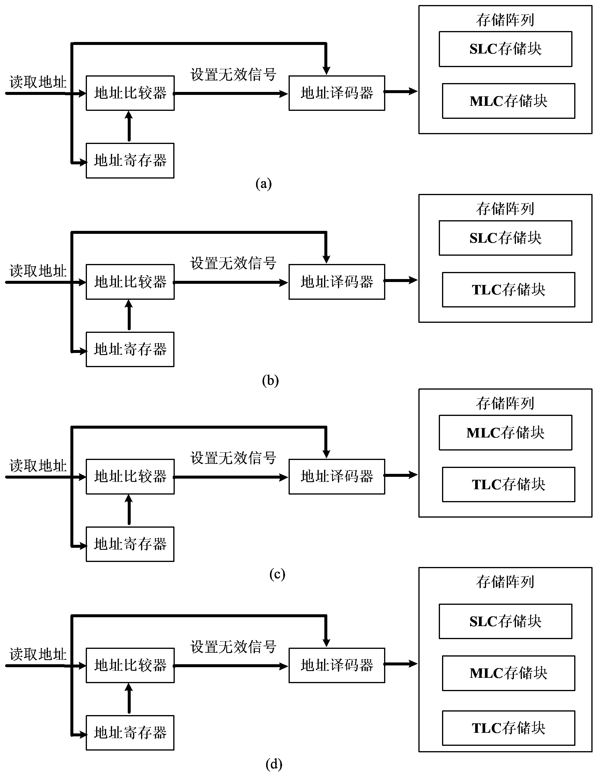
[0101] This embodiment provides a NAND Flash memory, the NAND Flash memory can freely configure the storage mode of each storage block, wherein the storage mode includes SLC mode, MLC mode and / or TLC mode. in:

[0102] SLC (Single-Level Cell, single-value unit), which represents a memory storage unit to store 1 bit, that is, 1bit / cell.

[0103] MLC (Mult i-Level Cell, multi-value storage unit) records multiple sets of bit information in a unit through different levels of voltage, and realizes multi-bit storage capacity in the storage unit, typically 2bit, that is, 2bit / cell, represented as 1 memory storage unit stores 2 bits, the speed and life can be well balanced, and the storage density of SLC is theoretically doubled. It is generally used in solid-state hard disks, mobile hard disks, and high-performance U disks.

[0104] TLC (Trinary-Level Cell, three-value storage unit) means that a memory storage unit can store 3 bits, that is, 3bit / cell. Using charges of diff...

Embodiment 2

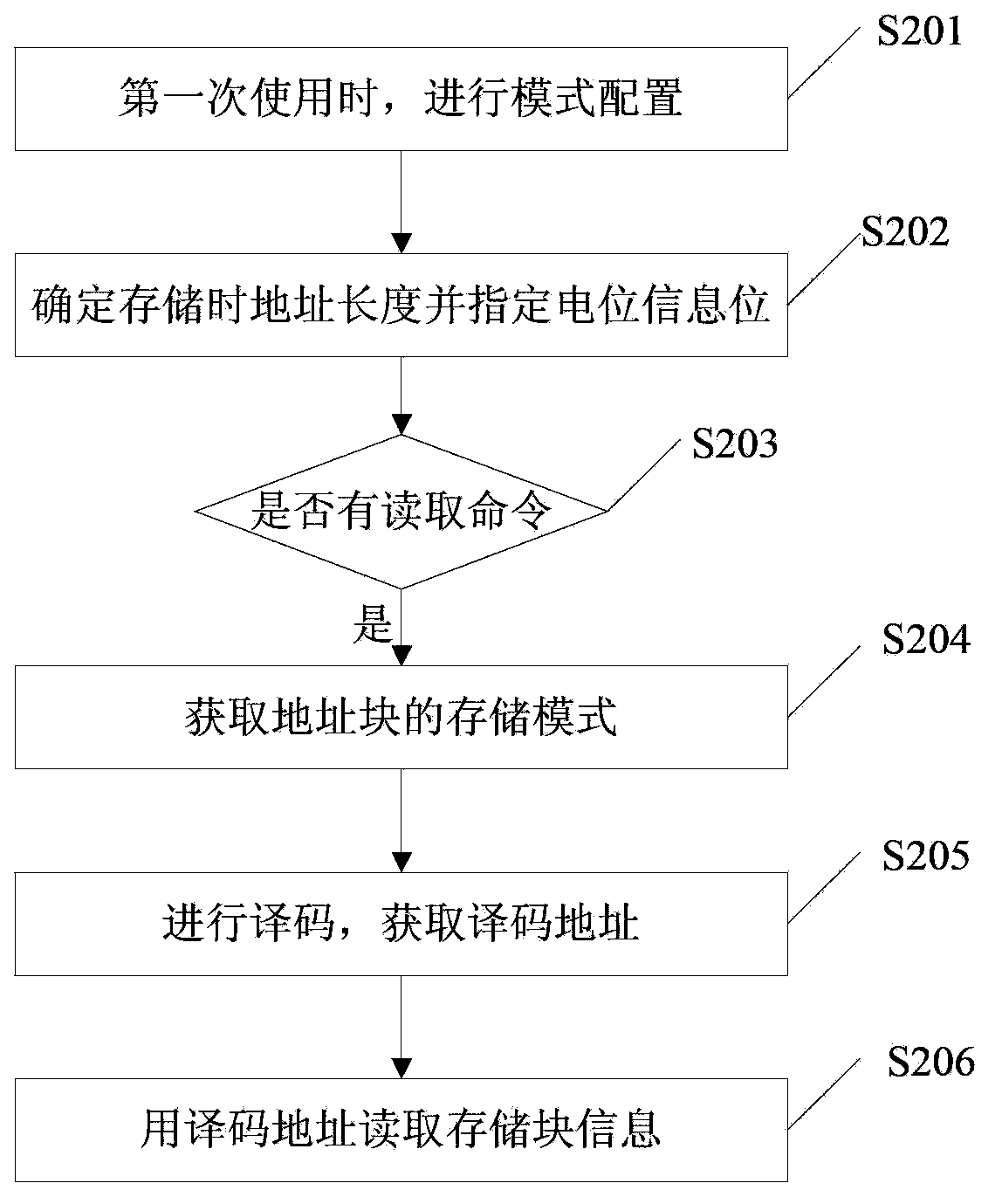
[0143] When the NAND Flash memory provided in this embodiment is used for the first time, the memory is set to a partial SLC mode and a partial MLC mode (that is, mode 4 in the above embodiment). An address list is established in the register for storing the addresses of the storage blocks in the MLC mode, and the addresses of the storage blocks set in the MLC mode are stored in the MLC list.

[0144] If you need to use n-bit address to locate the storage block, you need to use n+1-bit information to store the address of each storage block, and pre-designate one bit from the n+1-bit information to store the potential of the storage block in MLC mode information. Usually the first or last bit is designated to store the potential information of the memory block of the MLC mode

[0145] For example, if the last bit is specified to store the potential information of the memory block in MLC mode, the address of each memory cell is AD , where AD is specified to store the pot...

Embodiment 3

[0151] When the NAND Flash memory provided in this embodiment is used for the first time, the memory is set to a partial SLC mode, a partial MLC mode, and a partial TLC mode (that is, mode seven in the above embodiment). In the register, two address lists are respectively set up to be used to store the address of the storage block of the MLC mode and the address of the storage block of the TLC mode, and the address of the storage block that is set to the MLC mode is stored in the MLC list, and will be set as Addresses of memory blocks in TLC mode are stored in the TLC list.

[0152] If you need to use n-bit address to locate the storage block, you need to use n+2-bit information to store the address of each storage block, and pre-designate two bits for storing the potential of the storage block in TLC mode from the n+2-bit information information, further specifying one bit from the specified two bits to indicate invalid information when the storage block pointed to by the...


PUM


Abstract

The invention discloses an NAND Flash memorizer and an implementing method and system of the NAND Flash memorizer. The NAND Flash memorizer comprises a register, a comparator, an address decoder and a memory array; a memory mode and configuration information of the NAND Flash memorizer can be stored in the register in advance when the NAND Flash memorizer is used for the first time; the configuration of the memory mode comprises one mode of a partial SLC (Single Level Cell) mode and partial MLC (Multi Level Cell) mode, a partial SLC (Single Level Cell) mode and partial TLC mode, a partial MLC mode and partial TLC mode, and a partial SLC mode, partial MLC mode and partial TLC mode; the configuration information comprises an address of a memory block and the type of the memory block; the type of the memory block is an SLC type, an MLC type or a TLC type. According to the NAND Flash memorizer and the implementing method and system of the NAND Flash memorizer disclosed by the invention, the flexible configuration of each memory block can be realized and a plurality of types of memory modes are realized, so that the degree of freedom of the memorizer is high.

Description

technical field [0001] The invention relates to the technical field of data storage, in particular to a NAND Flash memory, a method for realizing the NAND Flash memory and a system thereof. Background technique [0002] Flash memory (flash memory, flash memory for short) is a new type of storage medium born in the late 1980s. Due to its excellent characteristics such as non-volatile, high speed, high shock resistance, low power consumption, small size and light weight, flash memory has been widely used in embedded systems and portable devices in the fields of mobile communication and data acquisition in recent years, such as mobile phones and portable media players. Devices, digital cameras, digital video cameras, sensors, and also used in aerospace and other fields, such as aerospace vehicles. [0003] Generally, a flash memory stores 1-bit data in one cell storing data "0" or "1". In order to achieve stronger storage capacity than this and higher density storage, two or ...

Claims


Application Information

Patent Timeline
IPC IPC(8): G11C16/02G11C16/06
Inventor 苏志强舒清明丁冲张君宇
Owner GIGADEVICE SEMICON (BEIJING) INC
Why Eureka
Try Eureka