Wafer pre-alignment method and device

A pre-alignment, wafer technology, used in electrical components, semiconductor/solid-state device manufacturing, circuits, etc., can solve problems such as reduced efficiency, wafer pre-alignment errors, and difficulty in ensuring accuracy, reducing measurement data, eliminating Principle error, the effect of eliminating error

Active Publication Date: 2016-12-21
SHENYANG SIASUN ROBOT & AUTOMATION
View PDF9 Cites 0 Cited by
  • Summary
  • Abstract
  • Description
  • Claims
  • Application Information

AI Technical Summary

Problems solved by technology

[0003] The traditional wafer pre-alignment method based on linear array CCD requires that the line where the CCD array is located passes through the rotation center of the wafer, but this accuracy is difficult to guarantee in practical applications. The relative position relationship of the wafer rotation axis, which will bring errors to the wafer pre-alignment; and the traditional wafer pre-alignment method, for the detection of the center position of the wafer, it often needs to make the wafer rotate a circle to obtain the wafer Although complete edge information increases the amount of data, it does not improve the acquisition accuracy of the data itself, so the accuracy of wafer pre-alignment cannot be significantly improved, and the efficiency is also reduced; in addition, traditional wafer pre-alignment The accurate method is to collect information in real time during the rotation of the wafer. It is impossible to accurately correspond the information of the edge of the wafer collected by the CCD sensor with the information of the corner of the wafer measured by the motor encoder. Pre-alignment introduces errors

Method used


Image

  • Wafer pre-alignment method and device
  • Wafer pre-alignment method and device
  • Wafer pre-alignment method and device

Examples


Embodiment Construction

[0053] In order to make the object, technical solution and advantages of the present invention clearer, the present invention will be further described in detail below in conjunction with the accompanying drawings and embodiments. It should be understood that the specific embodiments described here are only used to explain the present invention, not to limit the present invention.

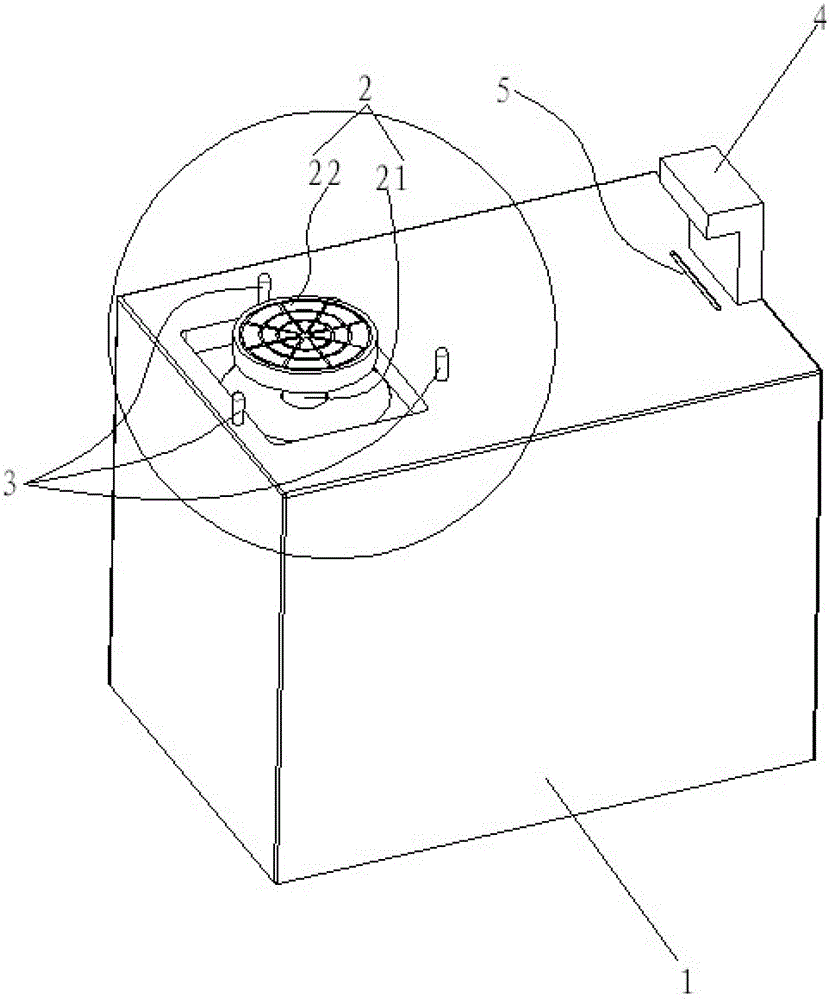
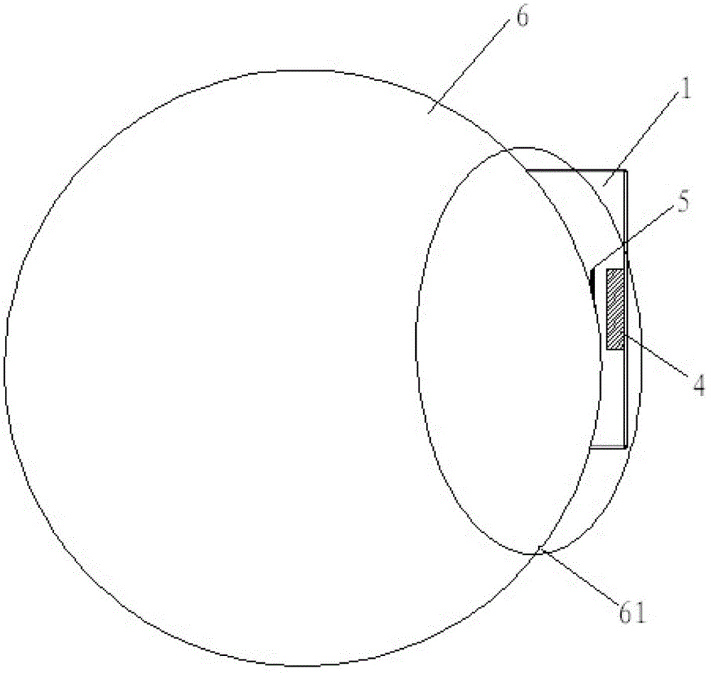
[0054] refer to figure 1 As shown, the present invention discloses a wafer pre-alignment device, which includes: a base 1, a suction cup assembly 2, a support assembly 3, a light source 4, and a CCD sensor 5, wherein:

[0055] The machine base 1 is provided with a driving device and a mechanism, which can drive the suction cup assembly 2 to rotate around its center line for lifting movement, and can also translate along the X and Y axes of the coordinate system.

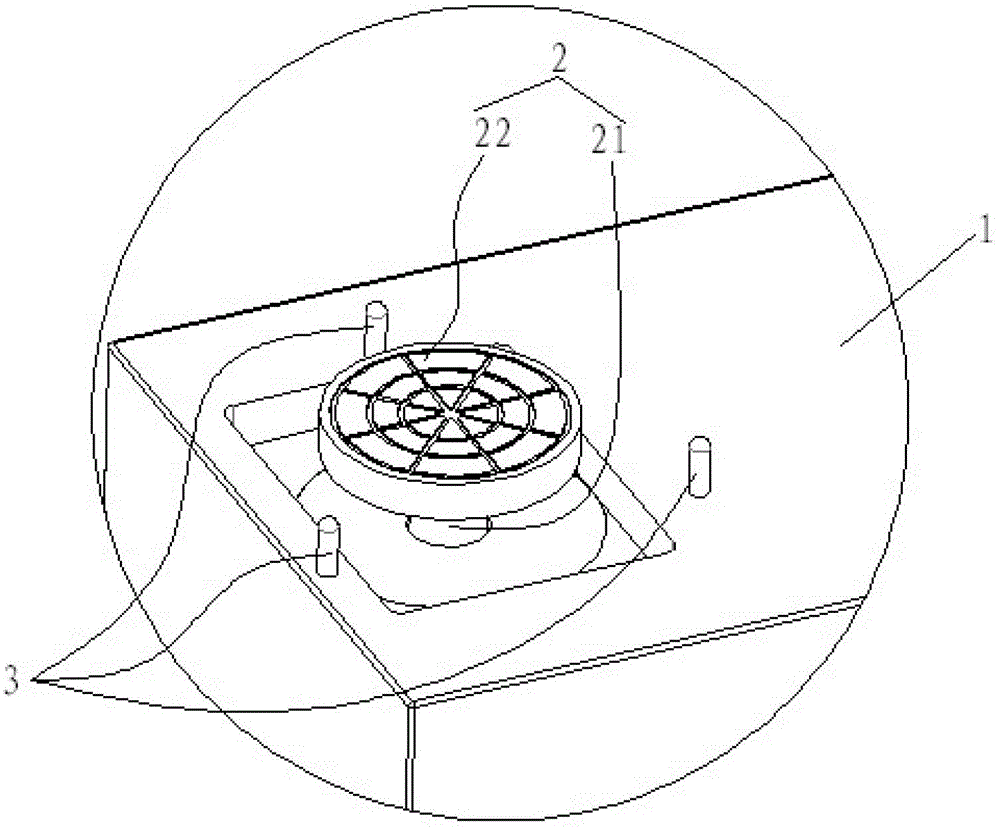
[0056] Cooperate figure 2 , 3 As shown, the suction cup assembly 2 includes a suction cup shaft 21 and a suction cup contact unit 22...


PUM


Abstract

The invention discloses a wafer pre-alignment method and apparatus. The apparatus is composed of a base, a sucking plate assembly, a support assembly, a light source, and a charge coupled device (CCD) sensor. A drive device and mechanism is arrange in the base and can drive the sucking plate assembly to make lifting motion, rotation or translation; the support assembly is arranged at the base and particularly, is arranged round the sucking plate assembly; the light source and the CCD sensor are arranged at the base; and the light source can project parallel lights to the CCD sensor. With the apparatus and the pre-alignment method, on the one hand, a principle error caused by an uncertain relative position of a wafer rotating shaft and a CCD line array can be eliminated; and on the other hand, static detection of the wafer decentration can be realized and an error caused by measuring system delay can be eliminated. Moreover, measuring data are reduced and the wafer pre-alignment efficiency can be improved.

Description

technical field [0001] The present invention relates to the technical field of identifying wafer eccentricity and gaps, in particular to a wafer pre-alignment method and device. Background technique [0002] CCD (ChargeCoupledDevice), charge-coupled device, is a new type of semiconductor integrated optoelectronic device developed in the early 1970s. CCD devices are divided into two types: linear array CCD and area array CCD according to the arrangement of their photosensitive units. [0003] The traditional wafer pre-alignment method based on linear array CCD requires that the line where the CCD array is located passes through the rotation center of the wafer, but this accuracy is difficult to guarantee in practical applications. The relative position relationship of the wafer rotation axis, which will bring errors to the wafer pre-alignment; and the traditional wafer pre-alignment method, for the detection of the center position of the wafer, it often needs to make the waf...

Claims


Application Information

Patent Timeline
Patent Type & Authority Patents(China)
IPC IPC(8): H01L21/68
CPCH01L21/681
Inventor 曲道奎李学威张鹏柴源何元一温燕修
Owner SHENYANG SIASUN ROBOT & AUTOMATION
Why Eureka
Try Eureka