Astronavigation FPGA universal refresh circuit based on JTAG interface and achieving method thereof

An implementation method and circuit technology, applied in the direction of logic circuits using specific components, logic circuits using basic logic circuit components, etc., can solve problems such as internal function disorder, short-circuiting, functional failure, etc., to achieve complete state and improve reliability. Strong and practical effect

Active Publication Date: 2014-06-04
BEIJING MXTRONICS CORP +1
View PDF7 Cites 8 Cited by
  • Summary
  • Abstract
  • Description
  • Claims
  • Application Information

AI Technical Summary

Problems solved by technology

This effect is the spatial single event flipping effect. The flipping of the configuration bit state may lead to serious functional failures, resulting in inter...

Method used


Image

  • Astronavigation FPGA universal refresh circuit based on JTAG interface and achieving method thereof
  • Astronavigation FPGA universal refresh circuit based on JTAG interface and achieving method thereof
  • Astronavigation FPGA universal refresh circuit based on JTAG interface and achieving method thereof

Examples


Embodiment 1

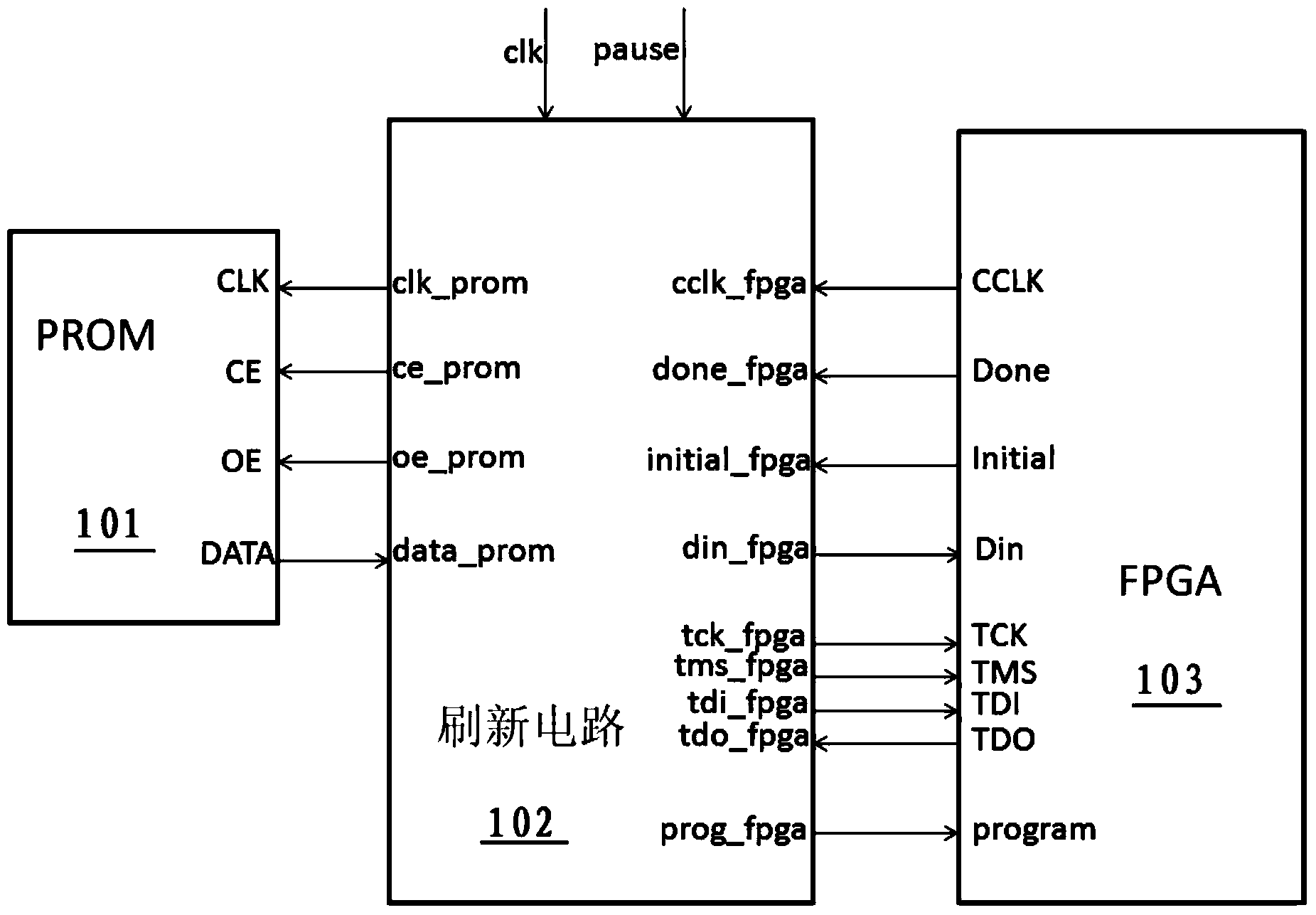
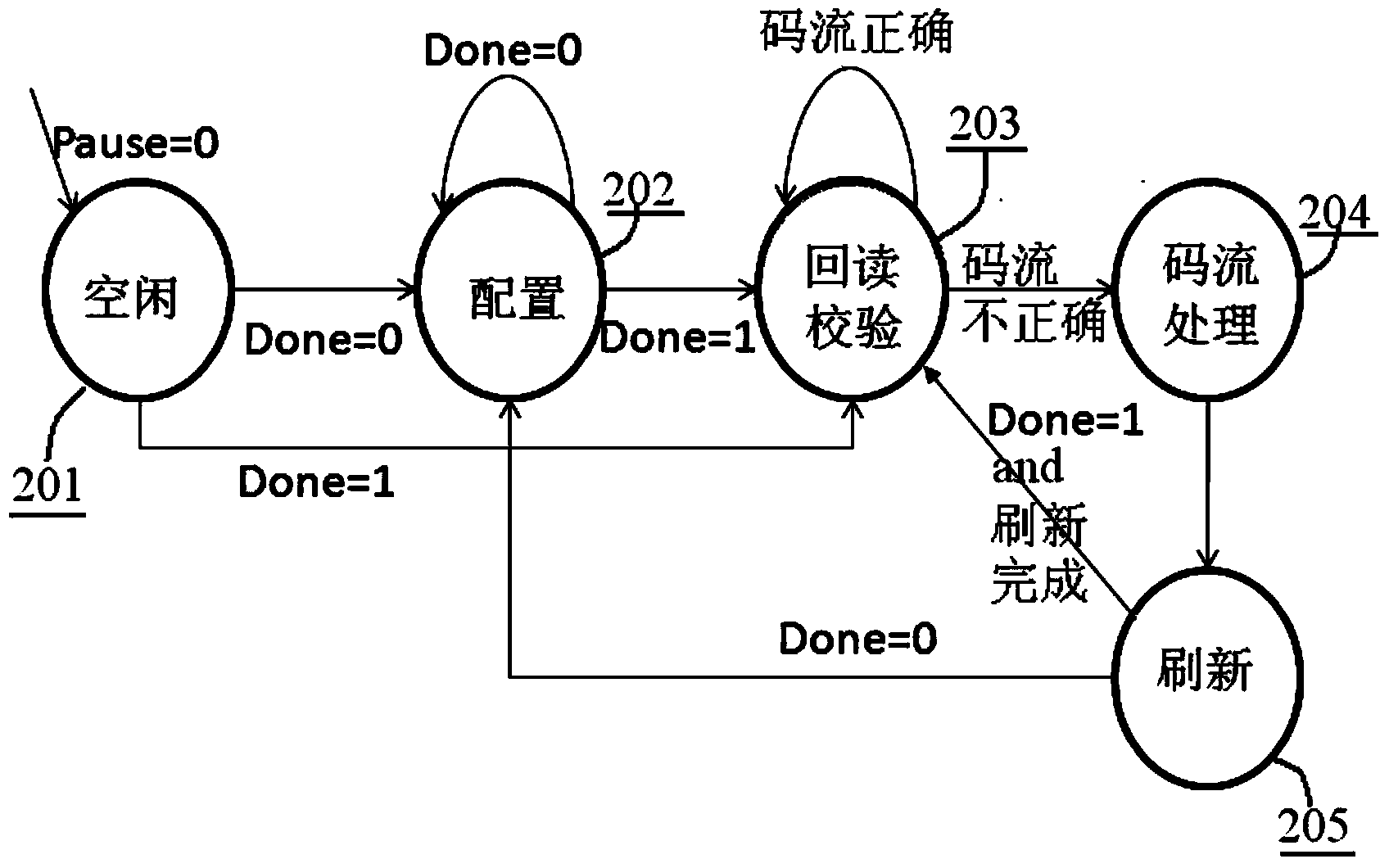
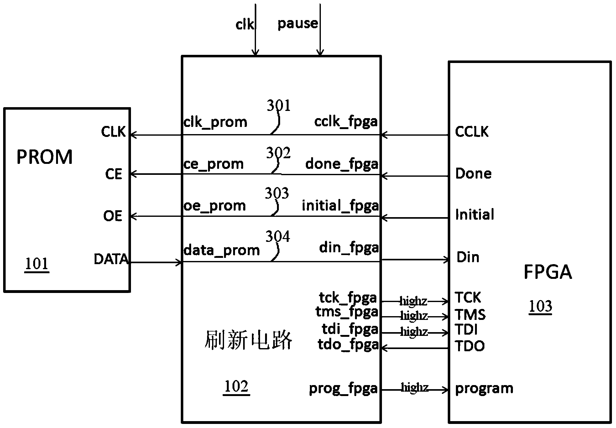
[0068] After power-on, connect the pause pin of the refresh circuit 102 to "0" level, then the refresh circuit 102 suspends work, enters and remains in the idle state 201; when the refresh circuit is in the idle state, if image 3 , connect the internal connections 301, 302, 303, 304, and connect the corresponding pins of PROM101 and FPGA103 together, that is, the CLK pin of PROM101 is connected to the CCLK pin of FPGA103, the CE pin of PROM101 is connected to the Done pin of FPGA103, The OE pin of PROM101 is connected to the Initial pin of FPGA103, and the DATA pin of PROM101 is connected to the Din pin of FPGA103; at the same time, the outputs of tck_fpga, tdi_fpga, tms_fpga and prog_fpga of refresh circuit 102 are in a high-impedance state. At this time, the refresh circuit 102 has no influence on the PROM 101 and the FPGA 103 , and it can be regarded that the refresh circuit 102 is bypassed.

Embodiment 2

[0070] After power-on, the pause pin of the refresh circuit 102 is connected to “1” level, the clk pin is connected to a clock signal with a fixed frequency, and the input signal of the done_fpga pin is started to be detected. If the refresh circuit 102 detects that the done_fpga level is “0”, the refresh circuit 102 will enter the configuration state 202 , otherwise it will directly jump to the readback verification state 203 . In configuration state 202, such as image 3 , the refresh circuit 102 is connected to the internal connections 301, 302, 303, 304, and the corresponding pins of the PROM101 and FPGA103 are connected together, that is, the CLK pin of the PROM101 is connected to the CCLK pin of the FPGA103, and the CE pin of the PROM101 is connected to the Done pin of the FPGA103. Pins, the OE pin of PROM101 is connected to the Initial pin of FPGA103, the DATA pin of PROM101 is connected to the Din pin of FPGA103; during the FPGA configuration process, the Done pin outp...


PUM


Abstract

The invention relates to an astronavigation FPGA universal refresh circuit based on a JTAG interface. The refresh circuit is provided with seven input pins and eight output pins, and the input pins and the output pins are connected with pins of a PROM and pins of an FPGA. The SRAM-type FPGA is subjected to backward reading operation through the JTAG interface, the type of the FPGA is determined, and backward read data are checked; if errors happen, a code stream is read from a correct data source, effective parts are intercepted from the code stream, the effective code stream is written into an inner configuration bit of the FPGA again through the JTAG interface, and accordingly refreshing of a configuration memory is completed. Through the refresh circuit, single event upset of the astronavigation FPGA can be timely detected and corrected, functional faults caused by single event upset of the astronavigation FPGA are eliminated, and astronavigation FPGA space application reliability is improved.

Description

technical field [0001] The invention relates to an aerospace FPGA general refresh circuit based on a JTAG interface and an implementation method thereof, in particular for detecting and recovering a space single-event flip fault occurring in an aerospace SRAM FPGA, and belongs to the technical field of integrated circuits. Background technique [0002] The basic structure of SRAM FPGA is as follows: Figure 5 , the main functional modules include: input and output modules (IOB) around the circle, two columns of block memory (Block RAM) on the edge, and internal programmable logic block array (CLB). In addition, there are connections throughout the entire circuit The interconnection resources of each module. The above logic resources and interconnect resources are all controlled by the underlying SRAM configuration bits. A large number of SRAM configuration bits all over the FPGA circuit determine the specific functions of the FPGA circuit, and the set of bit streams of thes...

Claims


Application Information

Patent Timeline
IPC IPC(8): H03K19/177
Inventor 张帆陈雷赵元富文治平李学武张彦龙孙华波王硕尚祖宾冯长磊王岚施林彦君郑咸建
Owner BEIJING MXTRONICS CORP
Why Eureka
Try Eureka