The realization method of aerospace fpga general refresh circuit based on selectmap

An implementation method and circuit technology, applied in the direction of logic circuits using basic logic circuit components, logic circuits using specific components, etc., can solve problems such as internal function disorder, connection short circuit, function failure, etc., to achieve a complete state and improve the circuit Reliable, practical results

Active Publication Date: 2017-01-04
BEIJING MXTRONICS CORP +1
View PDF4 Cites 1 Cited by
  • Summary
  • Abstract
  • Description
  • Claims
  • Application Information

AI Technical Summary

Problems solved by technology

This effect is the spatial single event flipping effect. The flipping of the configuration bit state may lead to serious functional failures, resulting in internal functional disorder, short circuit, open circuit, etc.
Faults caused by this configuration bit flip are permanent and can only be removed by reloading the bitstream

Method used


Image

  • The realization method of aerospace fpga general refresh circuit based on selectmap
  • The realization method of aerospace fpga general refresh circuit based on selectmap
  • The realization method of aerospace fpga general refresh circuit based on selectmap

Examples


Embodiment 1

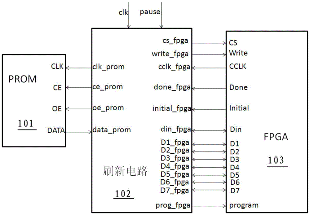
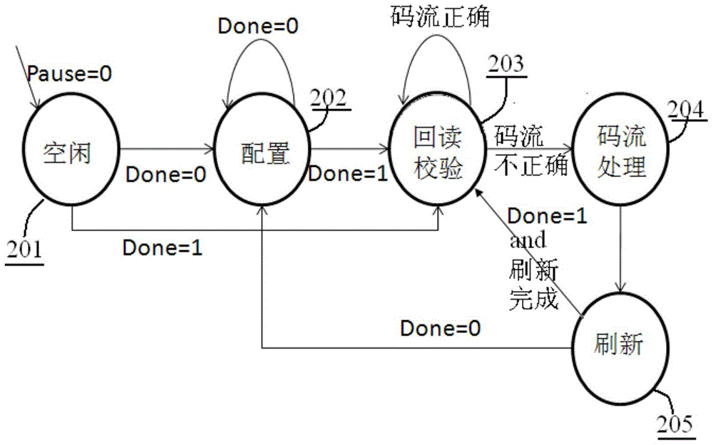
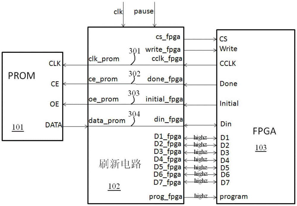
[0071] After power-on, connect the pause pin of the refresh circuit 102 to the "0" level, then the refresh circuit 102 suspends work, enters and remains in the idle state 201; in the idle state, the refresh circuit, such as image 3 Shown is a schematic diagram of the internal wiring and pin level of the refresh circuit of the present invention in the idle state, connecting the internal wiring 301, 302, 303, 304, and connecting the corresponding pins of PROM101 and FPGA103 together, that is, the CLK tube of PROM101 The pin is connected to the CCLK pin of FPGA103, the CE pin of PROM101 is connected to the Done pin of FPGA103, the OE pin of PROM101 is connected to the Initial pin of FPGA103, and the DATA pin of PROM101 is connected to the Din pin of FPGA103; at the same time, the refresh circuit 102 D1_fpga pins, D2_fpga pins, D3_fpga pins, D4_fpga pins, D5_fpga pins, D6_fpga pins, D7_fpga pins, cs_fpga pins, write_fpga pins, and prog_fpga output are in a high impedance state. At ...

Embodiment 2

[0073] After power-on, the pause pin of the refresh circuit 102 is connected to the "1" level, the clk pin is connected to a fixed-frequency clock signal, and the input signal of the done_fpga pin is detected. If the refresh circuit 102 detects that the done_fpga level is "0", the refresh circuit 102 will enter the configuration state 202, otherwise it will directly jump to the readback verification state 203. In the configuration state 202, such as image 3 , The refresh circuit 102 connects the internal wires 301, 302, 303, 304, and connects the corresponding pins of PROM101 and FPGA103, that is, the CLK pin of PROM101 is connected to the CCLK pin of FPGA103, and the CE pin of PROM101 is connected to Done of FPGA103. The OE pin of PROM101 is connected to the Initial pin of FPGA103, and the DATA pin of PROM101 is connected to the Din pin of FPGA103; in the FPGA configuration process, the Done pin of FPGA103 that has not been configured is output as "0" level. The CCLK pin will...


PUM


Abstract

The invention relates to an astronavigation FPGA universal refresh circuit based on SELECTMAP. The refresh circuit is provided with six input pins, six output pins and eight double-direction pins, and the input pins, the output pins and the double-direction pins are connected with pins of a PROM and pins of an FPGA. The SRAM-type FPGA is subjected to backward reading operation through SELECTMAP, the type of the FPGA is determined, and backward read data are checked; if errors happen, a code stream is read from a correct data source, effective parts are intercepted from the code stream, the effective code stream is written into an inner configuration bit of the FPGA again through SELECTMAP, and accordingly refreshing of a configuration memory is completed. Through the refresh circuit, single event upset of the astronavigation FPGA can be timely detected and corrected, functional faults caused by single event upset of the astronavigation FPGA are eliminated, and astronavigation FPGA space application reliability is improved.

Description

Technical field [0001] The invention relates to a SELECTMAP-based aerospace FPGA general refresh circuit and an implementation method thereof, and is particularly used for detecting and recovering a space single event flip failure of an SRAM FPGA for aerospace, belonging to the technical field of integrated circuits. Background technique [0002] The basic structure of SRAM FPGA Figure 5 , The main functional modules include: input and output modules (IOB) in a circle around, two rows of block memory (Block RAM), internal programmable logic block array (CLB), in addition to this, there are also connections throughout the circuit The interconnection resources of each module. The above-mentioned logic resources and interconnection resources are all controlled by the lower-level SRAM configuration bits. A large number of SRAM configuration bits distributed throughout the FPGA circuit determine the specific functions of the FPGA circuit, and the bit stream set of these configuration...

Claims


Application Information

Patent Timeline
Patent Type & Authority Patents(China)
IPC IPC(8): H03K19/177
Inventor 张帆陈雷赵元富文治平李学武张彦龙孙华波王硕尚祖宾冯长磊王岚施林彦君郑咸建
Owner BEIJING MXTRONICS CORP
Why Eureka
Try Eureka