Astronavigation FPGA universal refresh circuit based on SELECTMAP and achieving method thereof
An implementation method and circuit technology, applied in the direction of logic circuits using specific components, logic circuits using basic logic circuit components, etc., can solve problems such as internal function disorder, short-circuiting, functional failure, etc. Reliable, practical results
- Summary
- Abstract
- Description
- Claims
- Application Information
AI Technical Summary
Problems solved by technology
Method used
Image
Examples
Embodiment 1
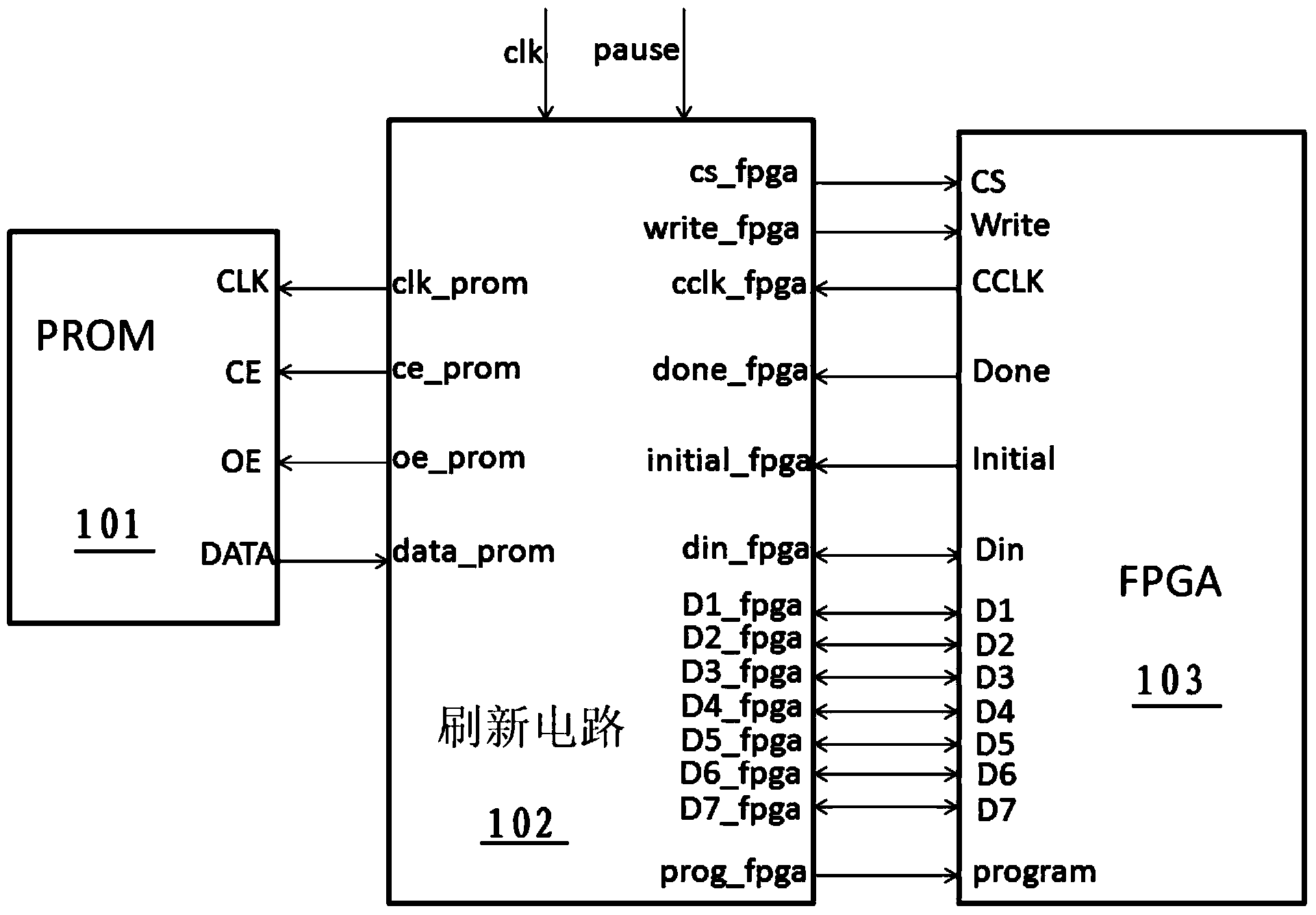
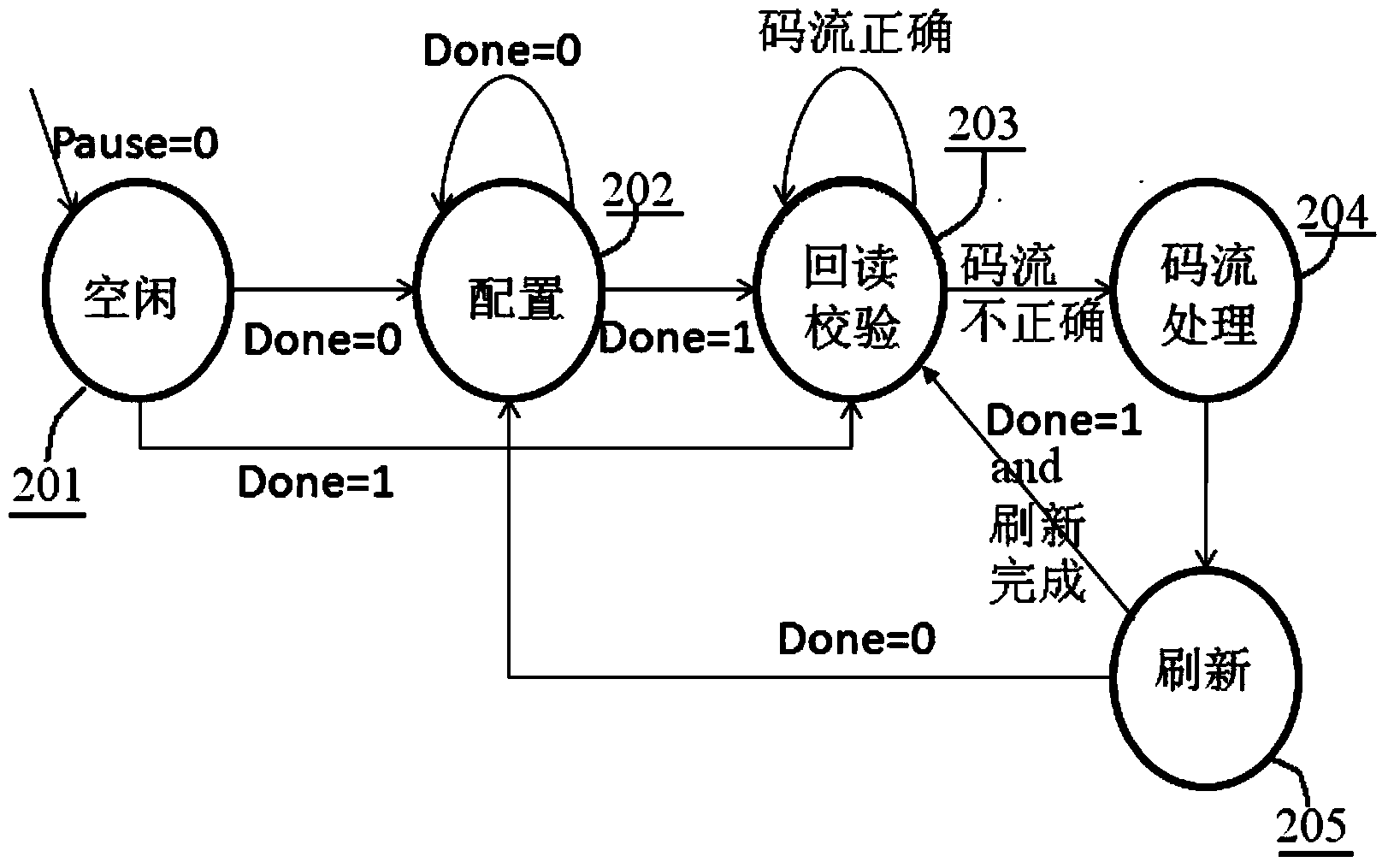
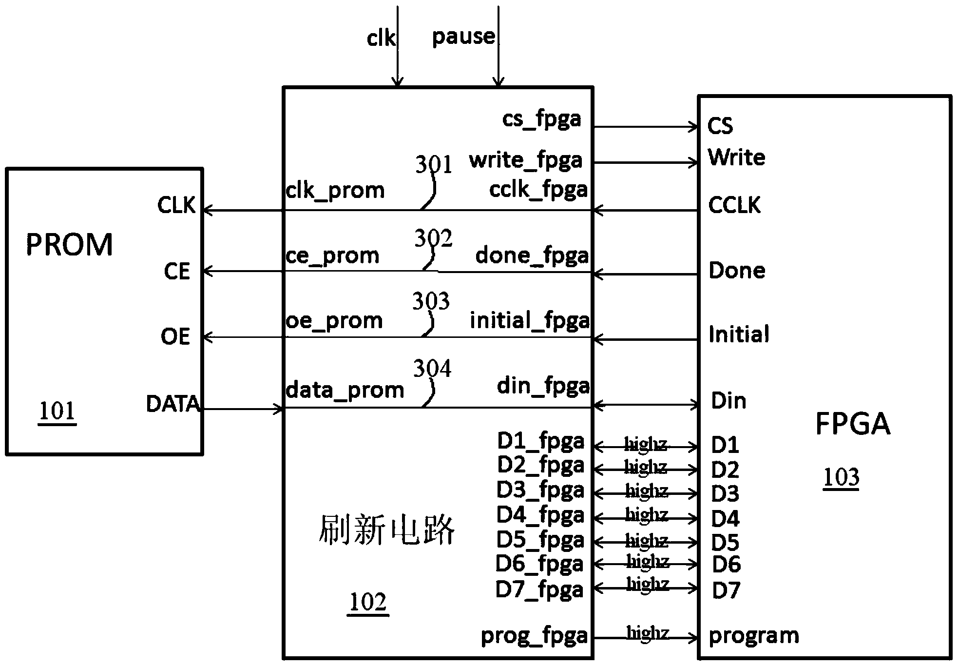
[0071] After power-on, connect the pause pin of the refresh circuit 102 to "0" level, then the refresh circuit 102 suspends work, enters and remains in the idle state 201; when the refresh circuit is in the idle state, if image 3 Shown is a schematic diagram of the internal wiring and pin levels of the refresh circuit of the present invention in an idle state. The internal wiring 301, 302, 303, and 304 are connected to connect the corresponding pins of the PROM101 and FPGA103 together, that is, the CLK tube of the PROM101 The pin is connected to the CCLK pin of FPGA103, the CE pin of PROM101 is connected to the Done pin of FPGA103, the OE pin of PROM101 is connected to the Initial pin of FPGA103, the DATA pin of PROM101 is connected to the Din pin of FPGA103; at the same time, the refresh circuit 102 D1_fpga pins, D2_fpga pins, D3_fpga pins, D4_fpga pins, D5_fpga pins, D6_fpga pins, D7_fpga pins, cs_fpga pins, write_fpga pins, and prog_fpga pins are high-impedance. At this ti...
Embodiment 2
[0073] After power-on, the pause pin of the refresh circuit 102 is connected to “1” level, the clk pin is connected to a clock signal with a fixed frequency, and the input signal of the done_fpga pin is started to be detected. If the refresh circuit 102 detects that the done_fpga level is “0”, the refresh circuit 102 will enter the configuration state 202 , otherwise it will directly jump to the readback verification state 203 . In configuration state 202, such as image 3 , the refresh circuit 102 is connected to the internal connections 301, 302, 303, 304, and the corresponding pins of the PROM101 and FPGA103 are connected together, that is, the CLK pin of the PROM101 is connected to the CCLK pin of the FPGA103, and the CE pin of the PROM101 is connected to the Done pin of the FPGA103. Pins, the OE pin of PROM101 is connected to the Initial pin of FPGA103, the DATA pin of PROM101 is connected to the Din pin of FPGA103; during the FPGA configuration process, the Done pin outp...
PUM
 Abstract
Description
Claims
Application Information


