A method for preparing thin films by dual-frequency magnetron sputtering based on radio frequency and very high frequency
A magnetron sputtering and very high frequency technology, which is applied in the field of thin film preparation by dual-frequency sputtering, can solve the problems of mutual interference of electric fields, double-target electric field coupling, and difficult independent control of sputtering, and achieve the effect of avoiding the phenomenon of electric field coupling
- Summary
- Abstract
- Description
- Claims
- Application Information
AI Technical Summary
Problems solved by technology
Method used
Image
Examples
Embodiment 1
[0025] Example 1 Ion energy distribution when preparing thin films by dual-frequency magnetron sputtering
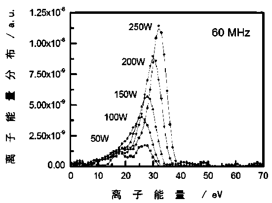
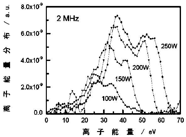
[0026] Adopting the dual-frequency sputtering film preparation method with independent control of ion energy provided by the present invention can realize the independent regulation of target sputtering energy during double-target sputtering, and realize partial decoupling of ion energy during sputtering. Through the ion energy distribution diagram Partial decoupling of sputtered ion energies can be seen.
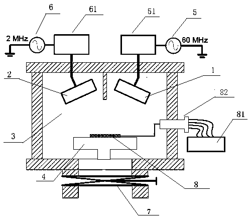
[0027] attached figure 1 It is a schematic diagram of the structure of the double-target magnetron sputtering device; according to the attached figure 1 The dual-frequency sputtering device includes a vacuum chamber 3, a sputtering target 1, a sputtering target 2, and a substrate table 4 installed on the top of the vacuum chamber at positions of 45° and 135° relative to the longitudinal symmetry axis of the vacuum chamber, respectively The 60MHz power supply 5 conne...
Embodiment 2
[0034] Embodiment 2 Preparation of SiC thin film by dual-frequency magnetron sputtering driven by radio frequency and very high frequency
[0035] The dual-frequency magnetron sputtering device in Embodiment 1 is used.
[0036] (1) Install the Si target and the C target required for preparing SiC thin films on the sputtering target 1 and the sputtering target 2 respectively;
[0037](2) Provide a (100)-oriented n-type silicon substrate (low-resistance single crystal silicon substrate), and perform standard cleaning; and place the cleaned substrate on the substrate stage in the vacuum chamber;
[0038] (3) Vacuum the vacuum chamber to 5×10 by turbomolecular pump and mechanical pump unit -4 Pa, then fill the vacuum chamber with argon, the flow of argon is 30sccm, and the pressure of the vacuum chamber is kept at 5Pa;
[0039] (4) Apply 60MHz VHF power to the Si target, adjust the VHF power to 150W, apply 2MHz RF power to the C target, adjust the RF power to 200W, and prepare S...
PUM
| Property | Measurement | Unit |
|---|---|---|
| diameter | aaaaa | aaaaa |
| diameter | aaaaa | aaaaa |
| particle size | aaaaa | aaaaa |
Abstract
Description
Claims
Application Information


