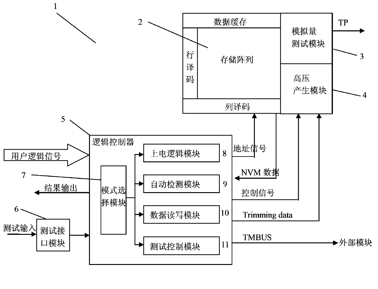
[0043] Such as figure 2 Shown is a schematic structural diagram of the non-volatile memory 1 of the embodiment of the present invention. The non-volatile memory 1 of the embodiment of the present invention includes a storage array 2, a test interface module 6, a high voltage generation module 4, an analog quantity test module 3, and a logic controller 5. It also includes row decoding, column decoding and data cache modules. The logic controller 5 includes: a mode selection module 7, a power-on logic module 8, a data reading and writing module 10, an automatic detection module 9 and a test control module 11.
[0044] The mode selection module 7 is used to generate a working state and a working mode of the non-volatile memory 1, the working state includes a user state and a test state; the working mode includes a power-on operation mode, a read operation mode, and a write operation Mode, test mode and automatic detection mode; the mode selection module 7 is jointly controlled by the user logic signal and the test input signal generated by the test interface module 6.
[0045] According to the working mode of the non-volatile memory 1, the power-on logic module 8 completes the sequential loading and automatic adjustment of the analog quantity from a specific area of the non-volatile memory 1 in the user state, and completes the In the test state, the analog quantity one is sequentially loaded from a specific area of the non-volatile memory 1, automatically adjusted, and the analog quantity one is loaded and single-step debugging in the adjustment process is performed, so that the non-volatile memory 1 It can work normally and stably after power-on. The analog quantity 1 loaded and adjusted by the power-on logic module 8 includes: the frequency of the clock oscillation module 24, the comparison current of the non-volatile memory 1, the voltage of the charge pump, and the voltage of the voltage calibration module 22. The specific area of the non-volatile memory 1 is a storage area of the storage array 2 dedicated to storing the analog quantity one loaded and adjusted by the power-on logic module 8.
[0046] Such as Figure 3A What is shown is a schematic structural diagram of a power-on logic module of a non-volatile memory in an embodiment of the present invention, and the power-on logic module 8 includes:
[0047] The clock oscillation (OSC) frequency adjustment module 12 is used to adjust the frequency of the clock oscillation module 24, and the clock oscillation frequency adjustment module 12 and the clock oscillation module 24 transmit frequency through a debug bus (TMBUS).
[0048] The comparison current adjustment module 13 is used to adjust the comparison current of the non-volatile memory 1. The comparison current adjustment module 13 generates the address and control signal of the storage array 2 and then reads the storage array 2 Compare the correction value of the current.
[0049] The calibration voltage adjustment module 14 is configured to adjust the calibration voltage of the voltage calibration module 22, and the calibration voltage is transmitted between the calibration voltage adjustment module 14 and the voltage calibration module 22 through a debugging bus.
[0050] The charge pump adjustment module 15 is used to adjust the charge pump voltage of the non-volatile memory. The charge pump adjustment module 15 generates the address and control signal of the storage array 2 and then reads the charge pump from the storage array 2 The correction value of the voltage.
[0051] The power-on logic module 8 starts to work after receiving the power-on operation enable, and outputs a signal Trdy after the power-on operation ends.
[0052] The test control module 11 controls the analog quantity test module 3 of the non-volatile memory 1 according to the working mode of the non-volatile memory 1, and completes the analog quantity including current and voltage under the test state. The second manual test, and the test result is output through the test output (TP) port; the analog quantity two includes two parts, the first part only needs to be adjusted and tested in the test mode, the second part is the analog quantity one, the The analog quantity one needs to be adjusted in the test mode and needs to be loaded when power is on. In the embodiment of the present invention, the test control module 11 completes the manual test of the analog quantity 2 including current and voltage in the test state by configuring the registers in the logic controller 5, and passes the non-volatile memory 1 The test output port outputs the result.
[0053] The automatic detection module 9 can detect the data information of the storage array 2 of the non-volatile memory 1, generate addresses and control signals of the non-volatile memory 1 in different configurations, and perform the operation of the storage array 2 Automatic comparison and detection of data, and return the detection result. Such as Figure 3B What is described is a schematic structural diagram of the automatic detection module 9 of the non-volatile memory of the embodiment of the present invention; the automatic detection module 9 starts to work under the control of the automatic detection mode enable signal, including:
[0054] The comparison configuration module 16 is used to configure the comparison mode and compare data.
[0055] The comparison address generating module 17 is used to generate the address and control signal of the non-volatile memory 1.
[0056] The detection module 18 is used to automatically compare and detect the data of the storage array 2. After the detection is successful, the detection module 18 will output the detection result; at the same time, the detection module 18 generates a comparison stop signal to the comparison address generation module 17 when a comparison error occurs, and stops the generation of addresses and control signals.
[0057] The data reading and writing module 10 generates the address of the non-volatile memory 1 according to the working mode of the non-volatile memory 1 and controls the high-voltage generating module 4 of the non-volatile memory 1 to complete the non-volatile memory 1. Read and write operations of volatile memory 1 data. Such as Figure 3C Shown is a schematic structural diagram of a data reading and writing module of a non-volatile memory according to an embodiment of the present invention; the data reading and writing module 10 starts to work under the control of a read operation enable signal or a write operation enable signal, including:
[0058] The read-write address generating module 19 is used to generate the read-write address of the storage array 2.
[0059] The read control module 20 and the write control module 21 are respectively used to generate control signals for read and write operations and to control the high voltage generation module 4.
[0060] Such as Figure 4 What is shown is a schematic diagram of the connection between the non-volatile memory and the external module in the embodiment of the present invention. The non-volatile memory 1 and the external module exchange data through a debug bus. The external modules include a clock oscillation module 24, a voltage calibration module 22, and a voltage detection module 23.
[0061] Such as Figure 5 As shown in the timing diagram of the debug bus in the embodiment of the present invention, the debug bus includes an external slow clock (SCK), a start flag signal (SRST) and a bidirectional data signal (SDIO). In the test mode, the adjustment of the analog quantity of the external module is completed by reading and writing the register, and the external logic responds to the command of the non-volatile memory through the response cycle.
[0062] The working state of the non-volatile memory 1 is controlled by an external control signal, and its working state can be divided into the following test state and user state.
[0063] Test status:
[0064] In the test state, the test input can control the working mode of the non-volatile memory 1 through the test interface module 6; when in the test state, the non-volatile memory 1 can be in all the above-mentioned working modes, namely the power-on operation mode and the read operation Mode, write operation mode, test mode and automatic detection mode, and can perform single-step debugging of test steps. At the same time, the logic controller 5 provides a status register to display the results of each test step.
[0065] Power-on operation mode: the frequency of the clock oscillation module 24, the reference current of the non-volatile memory 1, the comparison current, and the voltage of the voltage calibration module 22, can be automatically loaded and adjusted, and the logic controller 5 The status register indicates the automatic adjustment result of each analog quantity.
[0066] Read operation mode: continuous data reading can be realized, and the data reading interval can be set at the same time, which is convenient for debugging the data reading speed of the non-volatile memory 1.
[0067] Write operation mode: The non-volatile memory 1 can be controlled to perform erasing and programming control signals, and the time of high-voltage operation can be adjusted at the same time. The result of the writing operation can be displayed by the result output signal Busy.
[0068] Test mode: This mode provides a method to manually adjust the analog current and voltage value under test status. By reading and writing the internal registers of the logic controller 5, the calibration of the analog quantity of each module is completed, and the measurement is performed through the TP port. The adjusted calibration value, that is, the analog adjustment value (Trimming data) can be written into a specific area of the storage array 2, so as to load the Trimming data in other modes.
[0069] Automatic detection mode: Under various configurations, the data of non-volatile memory 1 can be read quickly and the automatic detection result is given. The detection result can be read out through the status register of the logic controller 5. The automatic detection mode includes multiple comparison methods such as row comparison, column comparison, and diagonal comparison of the storage array 2.
[0070] user status:
[0071] At this time, the user logic signal controls the working mode of the non-volatile memory 1. In the user state, the non-volatile memory 1 can work in a power-on operation mode and a read and write operation mode. In the power-on operation mode, the logic controller 5 can automatically complete the automatic loading and adjustment of the analog quantity when power-on, so that the chip is in a normal and stable working state. The user only needs to wait for the corresponding time and observe the power-on operation As a result, the signal Trdy is output. In the write operation mode, the logic controller 5 can automatically generate a signal to control the high voltage generation module 4, and indicate the result of the write operation through the result output signal Busy; in the read data mode, continuous data reading can be realized.
[0072] The present invention has been described in detail through specific embodiments above, but these do not constitute a limitation to the present invention. Without departing from the principle of the present invention, those skilled in the art can make many modifications and improvements, which should also be regarded as the protection scope of the present invention.