
Three-dimensional fan-out type wafer level package structure and manufacturing process

A wafer-level packaging, fan-out technology, used in semiconductor/solid-state device manufacturing, semiconductor/solid-state device components, semiconductor devices, etc., can solve problems such as difficulty, slip, and dislocation are difficult to control, and achieve improvement warping effect

Active Publication Date: 2014-06-25
江苏中科智芯集成科技有限公司
View PDF3 Cites 17 Cited by
  • Summary
  • Abstract
  • Description
  • Claims
  • Application Information

AI Technical Summary

Problems solved by technology

[0002] Three-dimensional fan-out wafer-level packaging can achieve the highest density of three-dimensional stacking, the smallest size, and greatly improve chip speed and low power consumption, but there are also certain defects
At present, it is very difficult to control the warpage of the fan-out packaging using the molding process. The solutions in the prior art are to reduce the warpage from the aspects of material properties and the final shape of the molding; It is also difficult to control the slip and shift caused by (EMC) expansion and contraction

Method used


Image

  • Three-dimensional fan-out type wafer level package structure and manufacturing process
  • Three-dimensional fan-out type wafer level package structure and manufacturing process
  • Three-dimensional fan-out type wafer level package structure and manufacturing process

Examples


Embodiment Construction

[0045] The present invention will be further described below in conjunction with specific drawings.

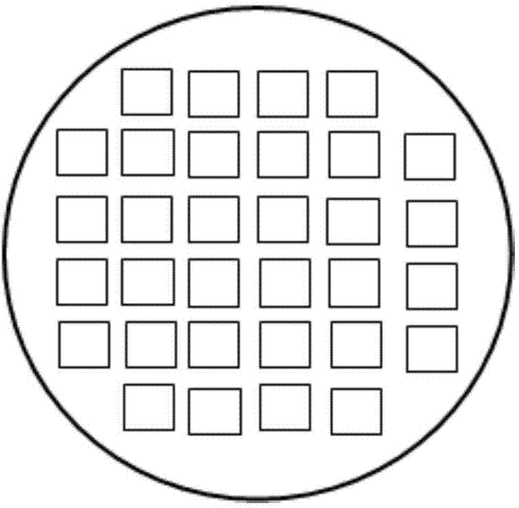
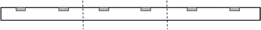
[0046] Such as Figure 18a , Figure 18b As shown, the three-dimensional fan-out wafer level packaging structure includes a first fan-out wafer level package body 10 and a second fan-out wafer level package body 20 (the first fan-out wafer level package body One, two, three or four layers of second fan-out wafer-level packages 20 can be stacked sequentially on top of 10, Figure 18a , Figure 18b Only one stack is shown);

[0047]The first fan-out wafer level package 10 includes a first chip 101 with metal electrodes 1011, 1012 and a first metal layer 102, the first chip 101 and the first metal layer 102 are plastic-sealed by a first plastic package 103 As a whole; the front 101a of the first chip 101 is located on the same plane as the front 103a of the first plastic package 103, the back 101b of the first chip 101 is located on the same plane as the back 103b of the firs...


PUM


Abstract

The invention relates to a three-dimensional fan-out type wafer level package structure and a manufacturing process. The manufacturing process is characterized in that metal layers are manufactured on a carrying sheet through the process with the front faces of chips facing upwards, grooving is conducted according to the arrangement positions of the chips, electrodes connected with other packaging units are manufactured according to the requirements, the internal structure of a fan-out type wafer level package is changed, rigidity is enhanced, the thermal coefficient of expansion is increased, and warping, slipping and dislocation of a whole wafer are reduced. Rerouting layer manufacturing is conducted on the front faces of the chips after plastic package is conducted, and bonding pads of the chips are fanned out to form first layer chip circuits. Then, the second layer chips are manufactured, the process with the front faces of the chips facing upwards is repeated, the corresponding chip and the corresponding metal layer are pasted on the first packaging unit, and the first packaging unit is connected with the previous packaging unit. Then, the plastic package process, drilling and metal filling are conducted. RDL manufacturing is conducted on the second layer chips. Finally, the multiple layers of chips are stacked by repeating the stacking process, or lower bump metal layers are manufactured on RDL layers, and the complete three-dimensional packaging structure is formed.

Description

technical field [0001] The invention relates to a three-dimensional fan-out wafer-level packaging structure and manufacturing process, belonging to the technical field of semiconductor packaging. Background technique [0002] The three-dimensional fan-out wafer-level packaging can achieve the highest stacking density in the three-dimensional direction, the smallest size, and greatly improve chip speed and low power consumption, but there are also certain defects. At present, it is very difficult to control the warpage of the fan-out packaging using the molding process. The solutions in the prior art are to reduce the warpage from the aspects of material properties and the final shape of the molding; It is also difficult to control the slippage and shift caused by (EMC) expansion and contraction. Contents of the invention [0003] The purpose of the present invention is to overcome the deficiencies in the prior art, and provide a three-dimensional fan-out wafer-level packa...

Claims


Application Information

Patent Timeline
IPC IPC(8): H01L23/538H01L23/31H01L21/768H01L21/56
CPCH01L24/19H01L2224/12105H01L2224/32145H01L2224/73267H01L2924/18162H01L2924/181H01L2224/94H01L2224/92244H01L2224/19H01L2924/00H01L2224/03H01L2924/00012
Inventor 王宏杰陈南南
Owner 江苏中科智芯集成科技有限公司
Learn More