esd protection structures, integrated circuits and semiconductor devices

A technology of ESD protection and integrated circuits, applied in semiconductor devices, electric solid state devices, circuits, etc., can solve the problems that devices are susceptible to ESD

Active Publication Date: 2017-01-04
INFINEON TECH AG
View PDF4 Cites 0 Cited by
  • Summary
  • Abstract
  • Description
  • Claims
  • Application Information

AI Technical Summary

Problems solved by technology

However, these highly scaled devices have been found to be increasingly susceptible to ESD

Method used


Image

  • esd protection structures, integrated circuits and semiconductor devices
  • esd protection structures, integrated circuits and semiconductor devices
  • esd protection structures, integrated circuits and semiconductor devices

Examples


Embodiment Construction

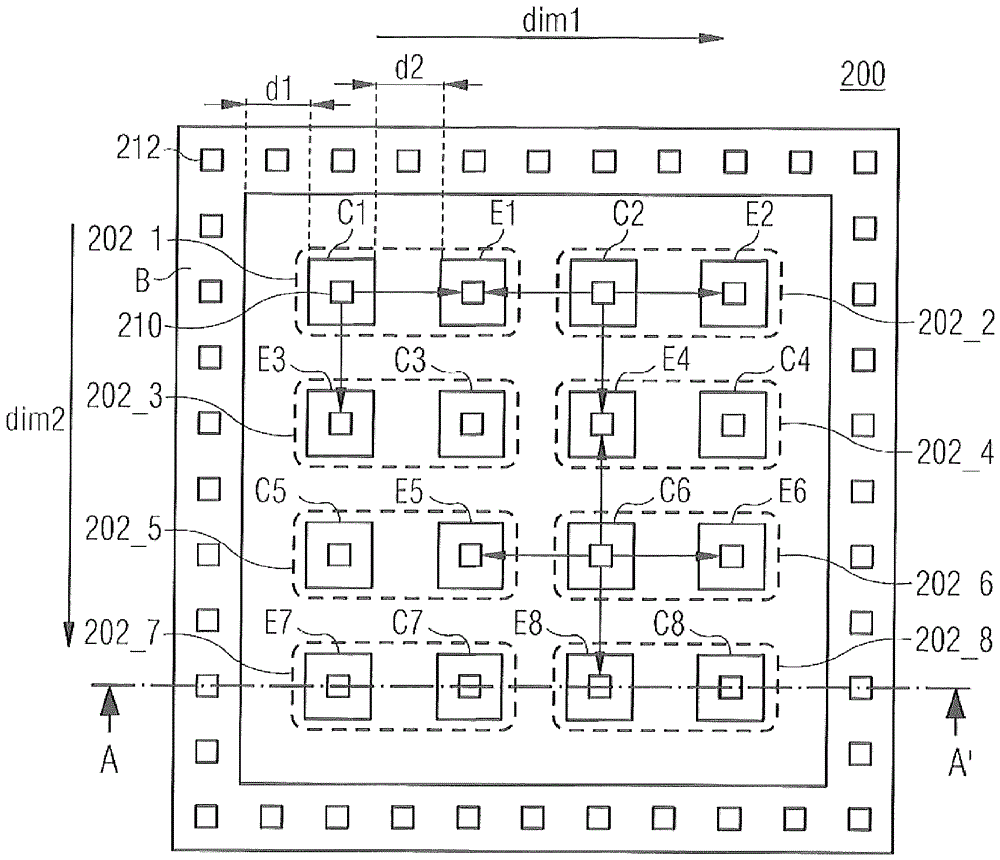
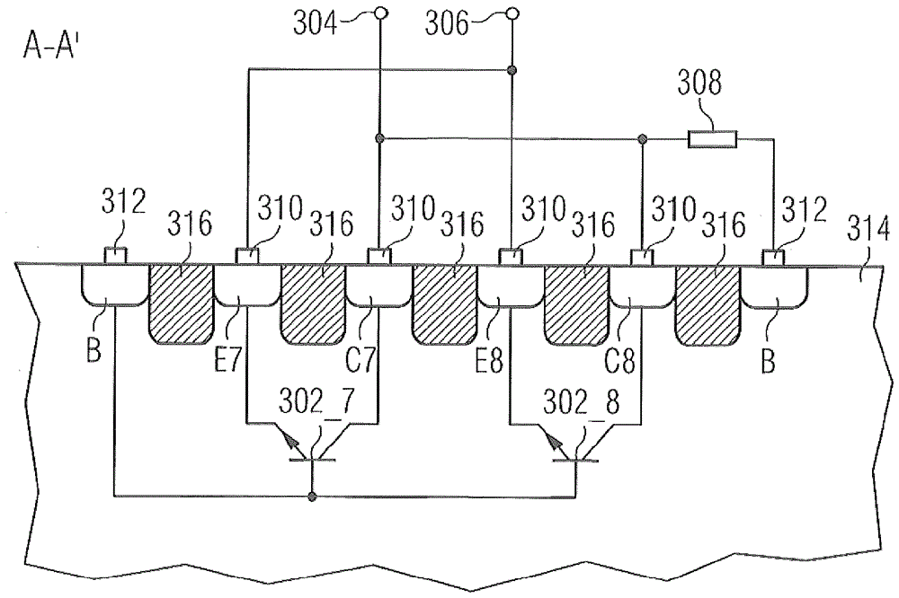
[0013] figure 1 A schematic circuit diagram of an exemplary ESD protection structure 100 comprising a plurality of transistors 102_1 , 102_2 . . . 102_n is shown. The plurality of transistors 102_1 , 102_2 . . . 102_n are all of the same type. together with figure 1 In the illustrated and described embodiment, the plurality of transistors 102_1 , 102_2 . . . 102_n are npn bipolar junction transistors (BJTs). The plurality of npn transistors 102_1 , 102_2 . . . 102_n are coupled in parallel, ie, the collector terminal C1 of the first transistor 102_1 , the collector terminal C2 of the second transistor 102_2 , and the collector terminal Cn of the nth transistor 102_n are coupled to each other. Furthermore, the emitter terminal E1 of the first transistor 102_1 , the emitter terminal E2 of the second transistor 102_2 , and the emitter terminal En of the nth transistor 102_n are coupled to each other. Furthermore, the base terminal B1 of the first transistor 102_1 , the base te...


PUM


Abstract

The present invention relates to ESD protection structures, integrated circuits and semiconductor devices. Embodiments including ESD protection structures are presented herein. The structure may include a plurality of first doped regions forming first terminals of a plurality of transistors, a plurality of second doped regions forming second terminals of the plurality of transistors, and surrounding the plurality of first doped regions. impurity region and the plurality of second doped regions to form a third doped region of the common third terminal of the plurality of transistors. The plurality of first doped regions and the plurality of second doped regions may be arranged in an alternating pattern such that an ESD discharge current received on any one of the plurality of first doped regions passes through the plurality of first doped regions. At least two of the second doped regions dissipate.

Description

Background technique [0001] Electrostatic discharge (ESD) protection design is a major factor in terms of integrated circuit reliability. In general, ESD is the transfer of electrostatic charge between subjects at different electrostatic potentials or voltages, either caused by direct contact or induced by an electrostatic field. In order to improve the transistor operating speed and the integration density of integrated circuits, the device dimensions of transistors of integrated circuits and the thickness of oxide and insulating layers are continuously reduced. However, it has been found that these highly scaled devices are increasingly susceptible to ESD. Therefore, ESD protection circuits have been added to integrated circuits to protect the integrated circuits from ESD damage. ESD protection circuitry can be implemented around the input, output, and power pads of an integrated circuit to shunt ESD current away from the internal devices of the integrated circuit. Descr...

Claims


Application Information

Patent Timeline
Patent Type & Authority Patents(China)
IPC IPC(8): H01L27/02
CPCH01L29/735H01L27/0259H01L29/73
Inventor K.多曼斯基
Owner INFINEON TECH AG
Why Eureka
Try Eureka