Display panel and display device

A technology of display panel and display area, applied in identification devices, instruments, nonlinear optics, etc., can solve the problems of affecting the quality of display images, degradation of display image quality, light leakage of flat panel displays, etc., so as to improve the quality of display images and avoid the problem of light leakage , the effect of improving quality

Active Publication Date: 2014-07-16
SHANGHAI TIANMA MICRO ELECTRONICS CO LTD +1
View PDF6 Cites 57 Cited by
  • Summary
  • Abstract
  • Description
  • Claims
  • Application Information

AI Technical Summary

Problems solved by technology

[0003] However, in actual use, it is found that there is an electrostatic problem in the flat panel display, which causes the quality of the display picture to decline, and there is also a light leakage problem in the flat panel display; both light leakage and static electricity have affected the quality of the display picture

Method used


Image

  • Display panel and display device
  • Display panel and display device
  • Display panel and display device

Examples


Embodiment 1

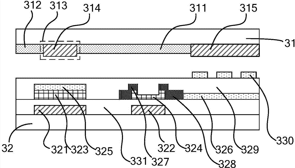
[0018] This embodiment provides a display panel, such as figure 1 with figure 2 As shown, it includes a display area and a non-display area surrounding the display area, and the display panel further includes: a first substrate 31 and a second substrate 32 oppositely arranged.

[0019] Wherein, the first substrate 31 includes on the side facing the second substrate 32: a first black matrix 311 located in the display area; a second black matrix 312 located in the non-display area; located between the first black matrix 311 and the second black matrix 312 Between the first slit 313, the first slit 313 disconnects the first black matrix 311 and the second black matrix 312, that is, the first slit 313 insulates the first black matrix 311 and the second black matrix 312 from each other.

[0020] The second substrate 32 faces the first substrate 31 on the side relative to the first substrate 31 from far to near, including in turn: a light shielding layer 321 and a light absorbing ...

Embodiment 2

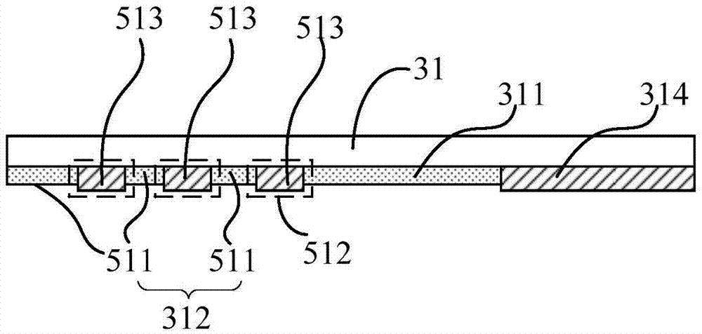
[0036] The present invention also provides another embodiment. The same parts of this embodiment as Embodiment 1 will not be repeated. The difference from Embodiment 1 is that image 3 As shown, the side of the first substrate 31 facing the second substrate (not shown) includes a first black matrix 311 and a second black matrix 312, wherein the first black matrix 311 is located in the display area, and the second black matrix 312 is located in the non- In the display area, the second black matrix 312 includes at least two third black matrices 511, a second slit 512 is included between two adjacent third black matrices 511, and two adjacent third black matrices 511 pass through the second slit 512 are insulated from each other, and the third black matrix 511 is insulated from the first black matrix 311 .

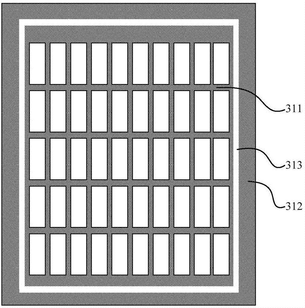
[0037] Such as image 3 The top view of the shown first substrate 31 along the direction perpendicular to itself can be shown as Figure 4 as shown in image 3 with Figu...

Embodiment 3

[0043] Based on the first and second embodiments above, an embodiment of the present invention provides a display device (not shown), including a display panel, and the display panel adopts the display panel described in the first and second embodiments.

[0044] The display device provided in this embodiment is not limited to a liquid crystal display device. On the premise that the core idea of ​​the present invention remains unchanged, the technical solution provided by the present invention is also applicable to an OLED (Organic Light-Emitting Diode, Organic Light-Emitting Diode) display device or electronic paper, etc.

[0045] To sum up, in the display panel and the display device provided by the embodiments of the present invention, the side of the first substrate facing the second substrate includes a first black matrix and a second black matrix, and the first black matrix is ​​located in the display area , the second black matrix is ​​located in the non-display area, a...


PUM


Abstract

The invention provides a display panel and a display device. The display panel comprises a first substrate and a second substrate which are arranged oppositely. A first black matrix and a second black matrix are formed on one face, facing the second substrate, of the first substrate, the first black matrix is positioned in a display area, the second black matrix is positioned in a non-display area, the first black matrix and the second black matrix are enabled to be disconnected by arranging a first slit between the same, a light shading layer and a light absorbing layer are sequentially arranged on one face, facing the first substrate, of the second substrate in a manner of being from far to near relatively to the first substrate, and shadows, of the light absorbing layer and the light shading layer, on the first substrate along a direction perpendicular to the first substrate cover the first slit. By the display panel and the display device, display picture quality can be improved.

Description

technical field [0001] The present invention relates to the field of display technology, in particular to a display panel and a display device. Background technique [0002] At present, flat panel displays, such as liquid crystal displays (Liquid Crystal Display, LCD) and organic light-emitting displays (OLED), are widely used in current flat panel displays due to their small size, light weight, thin thickness, low power consumption, and no radiation. dominated the market. [0003] However, in actual use, it is found that the flat panel display has a problem of static electricity, which causes the quality of the display picture to decline, and the flat panel display also has a problem of light leakage; both light leakage and static electricity affect the quality of the display picture. Contents of the invention [0004] In view of this, the present invention provides a display panel and a display device. [0005] The present invention provides a display panel, which incl...

Claims


Application Information

Patent Timeline
Patent Type & Authority Applications(China)
IPC IPC(8): G02F1/1335G09F9/33G09F9/30
Inventor 黄贤君丁洪
Owner SHANGHAI TIANMA MICRO ELECTRONICS CO LTD
Why Eureka
Try Eureka