Image sensor device and manufacturing method thereof

a technology of image sensor and manufacturing method, which is applied in the field of image sensor, can solve the problems of low spatial resolution and low photo sensitivity of image, and achieve the effects of low spatial resolution of image sensor, low photo sensitivity of image, and low spatial resolution

Active Publication Date: 2007-06-26
MARLIN SEMICON LTD
View PDF10 Cites 12 Cited by
  • Summary
  • Abstract
  • Description
  • Claims
  • Application Information

AI Technical Summary

Benefits of technology

[0007]Accordingly, the present invention is directed to an image sensor for preventing light leakage between different pixels to solve the problem of crosstalk. Thus, the spatial resolution and the photo sensitivity of the image sensor are enhanced.
[0008]In addition, the present invention is directed to a method of manufacturing an image sensor for preventing light leakage between different pixels to solve the problem of crosstalk. Thus, the spatial resolution and the photo sensitivity of the image sensor are enhanced.
[0027]Accordingly, in the present invention, since the non-transparent or reflective via walls are provided for preventing the light leakage between neighboring pixels, the problem of light leakage and crosstalk of the image sensor is solved. Therefore, the spatial resolution and the photo sensitivity of the image sensor are also enhanced. It is noted that, the image sensor of the invention may comprises one, two or more IMD layers, and the via walls may be disposed in any one or two or more IMD layers. The material of the via walls may be the same or different from the metal layers in the IMD. If the material of the via walls are identical to the metal layers, the via walls and the metal layers may be manufactured simultaneously. Therefore, the cost and the process time are not significantly increased.

Problems solved by technology

In a solid-state image sensor device, such as a CMOS image sensor described above, the problem of light leakage between different pixels is an important issue that may influence the photo sensitivity of the image sensor device. FIG. 1 is a cross-sectional view schematically illustrating a conventional image sensor device.
Therefore, the crosstalk between the pixels in the image sensor is generated and thus the spatial resolution of the image sensor is low.
Therefore, the photo sensitivity of the image is low.

Method used


Image

  • Image sensor device and manufacturing method thereof
  • Image sensor device and manufacturing method thereof
  • Image sensor device and manufacturing method thereof

Examples


Embodiment Construction

[0036]The present invention now will be described more fully hereinafter with reference to the accompanying drawings, in which preferred embodiments of the invention are shown. This invention may, however, be embodied in many different forms and should not be construed as limited to the embodiments set forth herein; rather, these embodiments are provided so that this disclosure will be thorough and complete, and will fully convey the scope of the invention to those skilled in the art. Like numbers refer to like elements throughout.

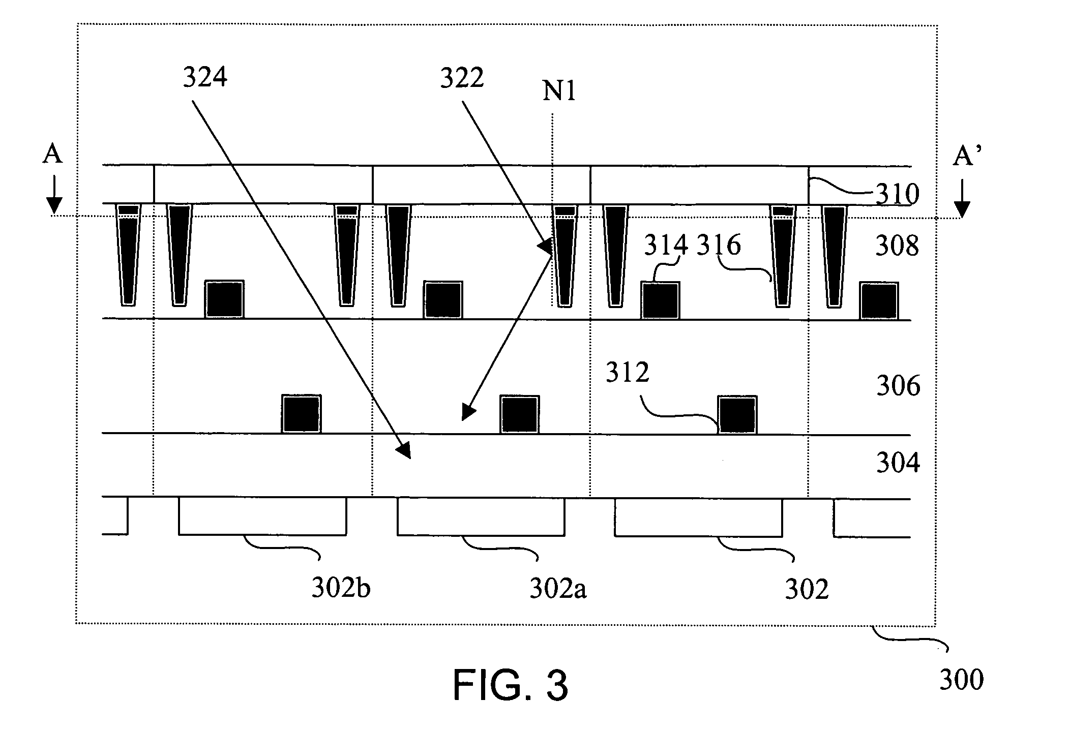
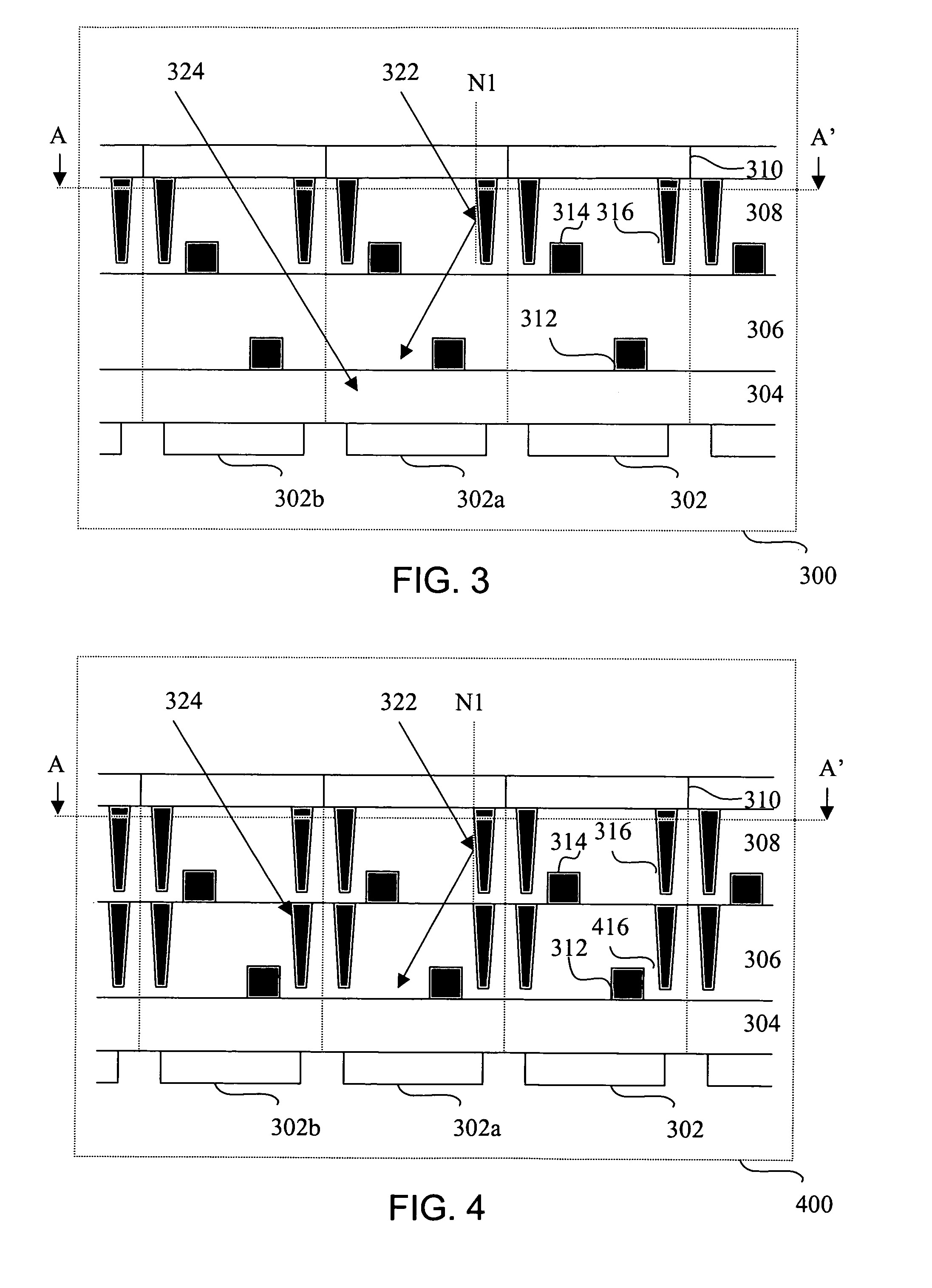
[0037]FIG. 3 is a cross-sectional view schematically illustrating an image sensor according to an embodiment of the present invention. Referring to FIG. 3, an image sensor 300 comprises, for example but not limited to, a plurality of sensors 302, an inter-layer dielectric (ILD) layer 304, inter-metal dielectric (IMD) layers 306 and 308 having a plurality of metal 1 (M1) layers 312 and metal 2 (M2) layers 314 respectively, a plurality of cover layers 310 an...


PUM


Abstract

An image sensor and a manufacturing method thereof are provided. The image sensor includes a plurality of sensors, an inter-layer dielectric layer formed over the sensors, a first inter-metal dielectric layer formed over the inter-layer dielectric layer, and a plurality of first via walls formed in the first inter-metal dielectric layer, wherein each of the first via walls is formed around each of the sensors. In addition, the image sensor further includes a second inter-metal dielectric layer formed over the first inter-metal dielectric layer and a plurality of second via walls formed in the second inter-metal dielectric layer, wherein each of the second via walls is formed around each of the sensors. Therefore, the light leakage between different pixels and the problem of crosstalk are solved, and the spatial resolution and the photo sensitivity of the image sensor are enhanced.

Description

BACKGROUND OF THE INVENTION[0001]1. Field of the Invention[0002]The present invention is generally related to an image sensor and a manufacturing method thereof. More particularly, the present invention relates to an image sensor and a manufacturing method thereof for preventing light leakage between different pixels.[0003]2. Description of Related Art[0004]Conventionally, a charge coupled device (CCD) is generally used for a solid-state image sensor since the property of high dynamic range, low dark current, and well developed technology. A conventional CCD comprises a photodiode array, and pulsed voltage is applied to the charge stored by each photodiode, so as to output a corresponding electric signal. However, in recent years, complementary metal oxide semiconductor (CMOS) image sensor (CMOS Image Sensor, “CIS”) is substantially developed for being compatible with the manufacturing process of a CMOS transistor. Thus, CMOS image sensor having a chip including a photodiode and an ...

Claims


Application Information

Patent Timeline
Patent Type & Authority Patents(United States)
IPC IPC(8): H01L29/15H01L21/00H01L27/146
CPCH01L27/14623H01L27/14625H01L27/14627H01L27/14643
Inventor CHEN, ANCHOR
Owner MARLIN SEMICON LTD
Why Eureka
Try Eureka