A method for fabricating self-aligned double-layer graphics with no load on the bottom
A manufacturing method and self-alignment technology, applied in semiconductor/solid-state device manufacturing, electrical components, circuits, etc., can solve problems such as damage to the bottom dielectric layer, loading effect at the bottom, and inability to remove the amorphous carbon film
- Summary
- Abstract
- Description
- Claims
- Application Information
AI Technical Summary
Problems solved by technology
Method used
Image
Examples
Embodiment Construction
[0039] In order to make the content of the present invention clearer and easier to understand, the content of the present invention will be further described below in conjunction with the accompanying drawings. Of course, the present invention is not limited to this specific embodiment, and general replacements known to those skilled in the art are also covered within the protection scope of the present invention.
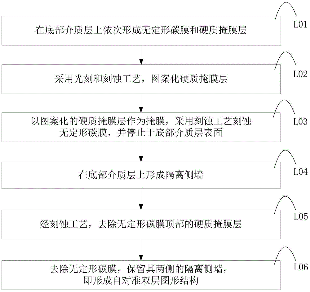
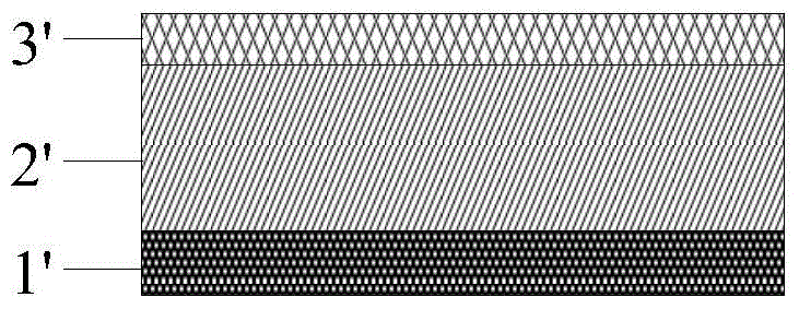
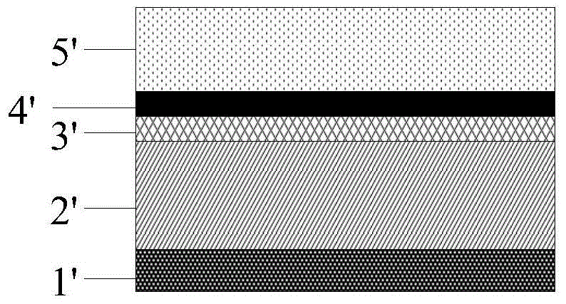
[0040] Below will combine specific embodiment and appended Figure 11-18 The method for fabricating the self-aligned double-layer pattern of the present invention will be further described in detail. Figure 11 It is a schematic flow chart of a method for fabricating a self-aligned double-layer pattern according to a preferred embodiment of the present invention, Figure 12-18 It is a schematic diagram of the cross-sectional structure formed by the specific steps of the method for fabricating the self-aligned double-layer pattern in the above-mentioned preferred e...
PUM
 Abstract
Description
Claims
Application Information


