OLED displayer, manufacturing method of OLED displayer and display device

A technology of display device and manufacturing method, which is applied to electric solid devices, semiconductor devices, electrical components, etc., can solve the problems of increasing device time and cost, reducing device transmittance, and cathode pixel disconnection, etc., so as to reduce the cost of cathode materials, The effect of increasing transmittance and uniform brightness

Active Publication Date: 2014-07-16
BOE TECH GRP CO LTD
View PDF8 Cites 39 Cited by
  • Summary
  • Abstract
  • Description
  • Claims
  • Application Information

AI Technical Summary

Problems solved by technology

But on the other hand, when depositing the cathode 250, the inverted trapezoidal PDL230 structure is easy to cause the fault of the cathode, thereby causing the cathode pixel open circuit defect, especially when the thickness of the cathode 250 is not enough to pave the pits between th

Method used


Image

  • OLED displayer, manufacturing method of OLED displayer and display device
  • OLED displayer, manufacturing method of OLED displayer and display device
  • OLED displayer, manufacturing method of OLED displayer and display device

Examples


Embodiment Construction

[0053] The specific implementation manners of the present invention will be further described in detail below in conjunction with the accompanying drawings and embodiments. The following examples are used to illustrate the present invention, but are not intended to limit the scope of the present invention.

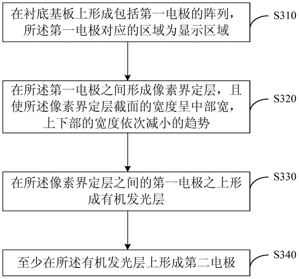
[0054] The invention provides a method for manufacturing an OLED display device, such as image 3 shown, including the following steps:

[0055] In step S310, an array including first electrodes is formed on the base substrate, and a region corresponding to the first electrodes is a display region.

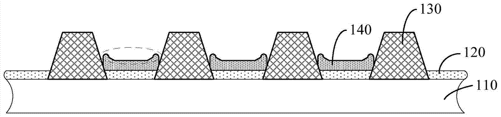
[0056] In step S320, a pixel defining layer is formed between the first electrodes, and the width of the section of the pixel defining layer is wider in the middle, and the width of the upper and lower parts decreases in turn.

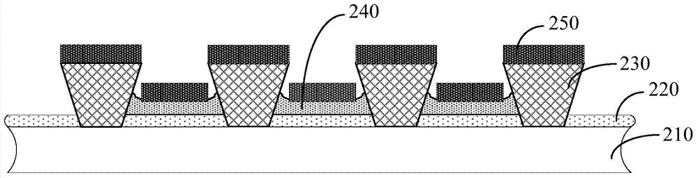
[0057] Step S330, forming an organic light emitting layer on the first electrode between the pixel defining layers.

[0058] Step S340, forming a s...


PUM

PropertyMeasurementUnit
Thicknessaaaaaaaaaa
Thicknessaaaaaaaaaa

Abstract

The invention relates to the technical field of displaying, and discloses a manufacturing method of an OLED displayer. The method includes the steps of forming an array comprising first electrodes on a substrate, wherein the areas corresponding to the first electrodes are display areas; forming pixel defining layers between the first electrodes, and enabling the widths of the cross sections of the pixel defining layers to be in the trend that the middles are wide, and the widths of the upper portions and the lower portions are successively reduced; forming organic luminous layers on the first electrodes between the pixel defining layers; at least forming second electrodes on the organic luminous layers. The invention further discloses the OLED displayer and a display device. According to the OLED displayer manufactured with the method, the coffee ring effects of the organic luminous layers are relieved to the greatest extent, faults of the second electrodes can be avoided, the display effect is accordingly improved, and materials of the second electrodes are saved.

Description

technical field [0001] The invention relates to the field of display technology, in particular to an OLED display device, a manufacturing method thereof, and a display device. Background technique [0002] Compared with LCD, organic electroluminescent device (OLED) has the advantages of self-luminescence, fast response, wide viewing angle, high brightness, bright color and thinness, and is considered to be the next generation display technology. [0003] The film-forming methods of OLED materials mainly include evaporation process and solution process. Evaporation process is relatively mature in small-scale applications. At present, this technology has been applied in mass production, and solution process OLED material film formation methods mainly include inkjet printing, nozzle coating, spin coating and screen printing. Among them, inkjet printing technology is considered to be an important way to achieve mass production of large-size OLEDs due to its high material utiliz...

Claims


Application Information

Patent Timeline
IPC IPC(8): H01L27/32
CPCH10K59/122H10K71/135H10K59/1201
Inventor 王辉锋
Owner BOE TECH GRP CO LTD
Why Eureka
Try Eureka