Power converter controller with multiple power sources
A technology of power converters and controllers, which is applied in the direction of output power conversion devices, conversion of DC power input to DC power output, and conversion equipment with intermediate conversion to AC, which can solve the problem of overall efficiency reduction and excessive power of power converters. Dissipation and other issues
Active Publication Date: 2014-07-23
POWER INTEGRATIONS INC
3 Cites 7 Cited by
AI-Extracted Technical Summary
Problems solved by technology
Using power supply circuit components of the power converter that are larger than the required voltage l...
Abstract
A controller includes a bypass terminal, a first power circuit, a second power circuit, and a charging control circuit. The bypass terminal is to be coupled to a bypass capacitor coupled to a secondary side of an isolated power converter. The first power circuit is coupled to the bypass terminal and a first terminal to be coupled to a first node of the secondary side. The first power circuit transfers charge from the first terminal to the bypass terminal for storage on the bypass capacitor. The second power circuit is coupled to the bypass terminal and a second terminal to be coupled to a second node of the secondary side. The second power circuit transfers charge from the second terminal to the bypass terminal for storage on the bypass capacitor. The charging control circuit controls which of the first and second power circuits transfers charge to the bypass terminal.
Application Domain
Efficient power electronics conversionApparatus with intermediate ac conversion +1
Technology Topic
Constant power circuitPower circuits +4
Image
Examples
- Experimental program(1)
Example Embodiment
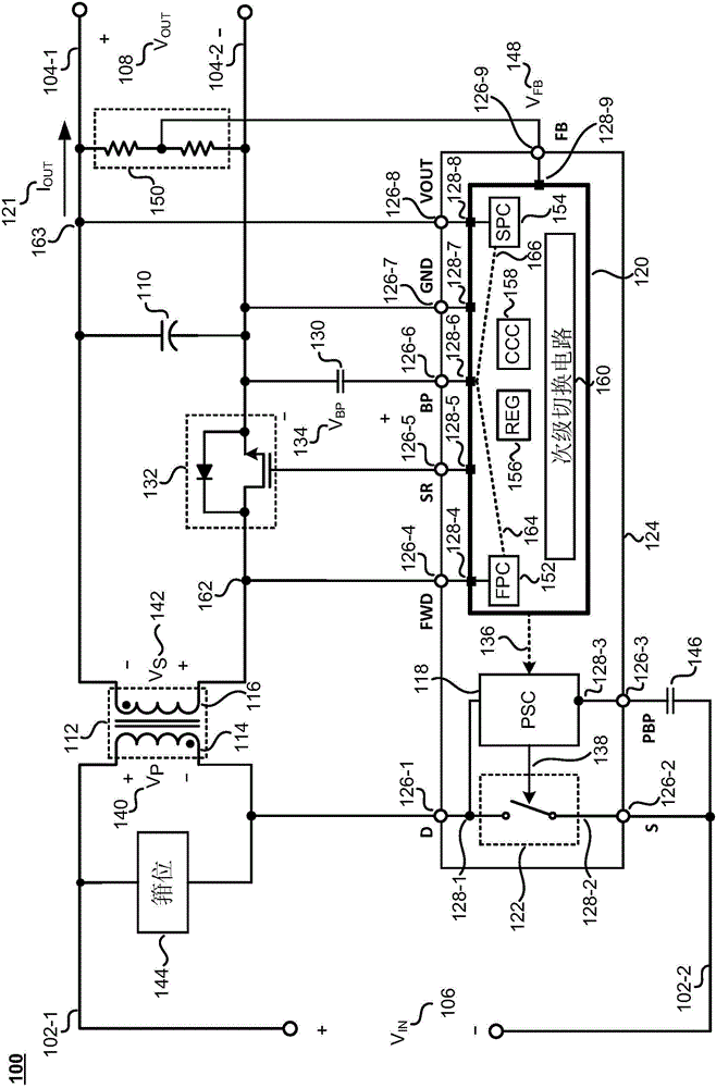
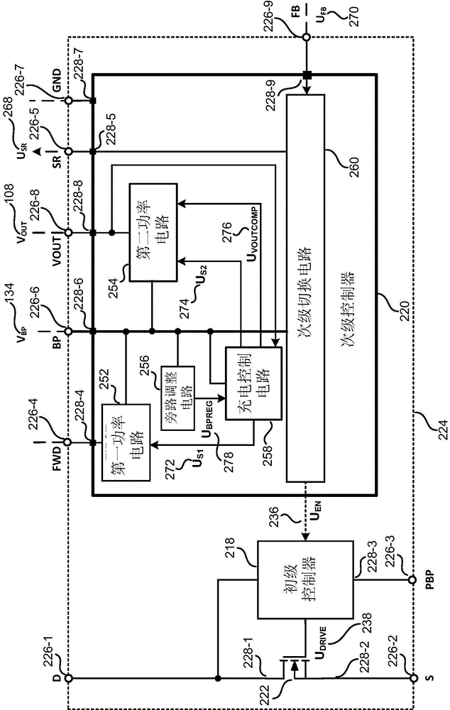
[0043] In the following description, numerous specific details are clarified to provide a thorough understanding of the present invention. However, those of ordinary skill in the art will understand that the specific details need not be adopted to practice the present invention. In other cases, well-known materials or methods are not described in detail to avoid obscuring the present invention.
[0044] Reference throughout this specification to "one embodiment", "an embodiment", "an example" or "an example" means that a specific feature, structure, or characteristic described in conjunction with the embodiment or example is included in this In at least one embodiment of the invention. Therefore, the phrases "in one embodiment", "in an embodiment", "one example" or "an example" appearing in various places throughout this specification do not necessarily all refer to the same embodiment or example. Furthermore, the specific features, structures or characteristics may be combined in any suitable combination and/or subcombination in one or more embodiments or examples. Specific features, structures, or characteristics may be included in integrated circuits, electronic circuits, combinational logic circuits, or other suitable components that provide the described functions. In addition, it should be appreciated that the figures provided here are for explanation to those of ordinary skill in the art, and these figures are not necessarily drawn to scale.
[0045] The isolated power converter according to the present disclosure includes a primary controller and a secondary controller that are galvanically isolated from each other by an energy transfer element (for example, a coupled inductor). In other words, the dc voltage applied between the input side and the output side will generate substantially zero current.
[0046] The primary controller is coupled to control the power switch on the primary side of the isolated power converter, thereby controlling the energy transfer from the primary winding of the energy transfer element to the secondary winding of the energy transfer element. The secondary controller is coupled to circuit components on the secondary side of the isolated power converter. Although the primary controller and the secondary controller are galvanically isolated from each other, the secondary controller can transmit a signal to the primary controller that controls how the primary controller switches the power switch to transfer energy to the primary controller. Secondary side.
[0047] The secondary side of the isolated power converter includes a bypass capacitor that provides operating power to the circuit of the secondary controller. The secondary controller of the present disclosure can charge the bypass capacitor from multiple nodes on the secondary side to adjust the bypass voltage across the bypass capacitor to a level sufficient to operate the circuit of the secondary controller . In one embodiment described herein, the secondary controller may charge the bypass capacitor from a first node connected to the secondary winding and a second node connected to the output of the isolated power converter.
[0048] The secondary controller may respond to a variety of different operating conditions (such as the magnitude of the bypass voltage and/or the magnitude of the output voltage at the second node) to select which of the first node and the second node is used. The bypass capacitor is charged. Generally speaking, when the output voltage at the second node is insufficient to charge the bypass capacitor to the adjusted bypass voltage, the secondary controller can use the first node to charge the bypass capacitor to the adjusted bypass voltage. Road voltage. When the output voltage at the second node is increased enough to charge the bypass capacitor to the adjusted bypass voltage, the secondary controller may transition from using the first node to using the second node.
[0049] During the startup of the isolated power converter, when the output voltage increases from an initial value of zero volts, the secondary controller may use the secondary winding voltage generated at the first node to charge the bypass capacitor. During startup, the secondary controller can use the secondary winding voltage because the output voltage of the isolated power converter can initially be at a level that is insufficient to charge the bypass capacitor. During startup, in response to the voltage generated at the secondary winding, the output voltage of the isolated power converter may increase. After a period of time, the output voltage of the isolated power converter increases to a level sufficient to charge the bypass capacitor. When the output voltage has reached a level sufficient to charge the bypass capacitor, the secondary controller may switch from using the first node to charge the bypass capacitor to using the second node to charge the bypass capacitor.
[0050] During the normal operation of the isolated power converter, the output voltage of the power converter can be adjusted to a level sufficient to charge the bypass capacitor. Therefore, during the normal operation of the isolated power converter, the secondary controller can continue to charge the bypass capacitor from the secondary node. However, in some cases, excessive loading at the output of the isolated power converter can cause the output voltage to drop to a level insufficient to charge the bypass capacitor. When the output voltage drops, the secondary controller can switch from using the second node to charge the bypass capacitor back to using the first node at the secondary winding to charge the bypass capacitor. Then, the secondary controller may transition back to using the second node to charge the bypass capacitor in response to the output voltage reaching a level sufficient to charge the bypass capacitor.
[0051] The ability of the secondary controller to select between multiple power sources can provide efficient bypass capacitor charging, because during the typical operation of the isolated power converter, the secondary controller can Charge from a relatively low voltage (for example, the output voltage). The ability to select between multiple power sources can also provide reliable charging of the bypass capacitor, because during operation, when the lower charging voltage (for example, the output voltage) of the isolated power converter drops , The secondary controller can switch to a higher charging voltage (for example, the secondary winding).
[0052] Refer now Figure 1-9 An exemplary isolated power converter according to the present disclosure is described. Figure 1-2 An exemplary isolated power converter is illustrated that includes a secondary controller that is coupled to a switch between multiple charging sources. Figure 3A , 3B And 4 show a method for operating the power converter of the present disclosure during startup and after the output voltage of the power converter has reached the desired adjusted output voltage. Figure 5-8 An exemplary circuit of the secondary controller is shown in more detail. Picture 9 The output voltage and bypass voltage during the operation of an exemplary power converter and the control signal of the secondary controller are illustrated.
[0053] figure 1 It is a schematic diagram of an exemplary power converter 100 according to the present disclosure. The exemplary power converter 100 is an isolated switch-mode power converter with a flyback topology. The power converter 100 includes input terminals 102-1 and 102-2 (collectively referred to as "input terminal 102") and output terminals 104-1 and 104-2 (collectively referred to as "output terminal 104"). The input terminal 102 is coupled to receive the input voltage V IN 106, input voltage V IN 106 may be a rectified and filtered ac voltage. For example, the input terminal 102 may be coupled to a full-bridge rectifier (not shown) and a filter capacitor (not shown), which are coupled to the ac voltage source The received ac voltage is rectified and filtered. In one embodiment, the input voltage V IN 106 may be a time-varying dc voltage. As shown, V IN 106. Taking the input terminal 102-2 as a reference, the input terminal 102-2 may be referred to as "input return 102-2".
[0054] The output terminal 104 will output the voltage V OUT 108 is provided to an electrical load (not shown), such as a tablet computer device. After the power converter 100 is started, the power converter 100 can reduce the output voltage V OUT The value of 108 is adjusted to the desired adjusted output voltage value (for example, 5-12Vdc). Start-up can be a period of time as follows, this time is introduced from the power converter 100 to V IN From 106 o'clock, until the control circuit of the power converter 100 starts to operate to adjust the output voltage V of the power converter 100 OUT 108. Therefore, the output voltage V OUT 108 can be referred to as "adjusted output voltage". The output terminal 104 is coupled to the output capacitor 110 to smooth out the adjusted output voltage V OUT 108. As shown, the output voltage V OUT With reference to output terminal 104-2, output terminal 104-2 may be referred to as "output return 104-2". In one embodiment, the output capacitor 110 may have a capacitance value in the range of approximately 200-600 μF.
[0055] As further shown, the power converter 100 includes an energy transfer element 112 that includes a primary winding 114 and a secondary winding 116. The energy transfer element 112 is coupled to transfer electrical energy from the primary coil 114 to the secondary coil 116. In one embodiment, the energy transfer element 112 may be a coupled inductor. The circuit electrically coupled between the input terminal 102 and the primary winding 114 may be referred to as the “primary side” of the power converter 100. The circuit electrically coupled between the secondary winding 116 and the output terminal 104 may be referred to as the “secondary side” of the power converter 100. The energy transfer element 112 provides galvanic isolation between the circuits on the primary side of the power converter 100 and the circuits on the secondary side of the power converter 100. Therefore, the dc voltage applied between the primary side and the secondary side of the power converter 100 will generate substantially zero current.
[0056] The power converter 100 includes a primary side control circuit 118 (hereinafter referred to as “primary controller 118”), a secondary side control circuit 120 (hereinafter referred to as “secondary controller 120”), and a power switch 122. The primary controller 118, the secondary controller 120, and the power switch 122 are included in an integrated circuit package 124, and the integrated circuit package 124 is figure 1 Is exemplified as a box.
[0057] In one embodiment, the integrated circuit package 124 may include a first integrated circuit die and a second integrated circuit die within an encapsulation. The encapsulant may refer to an encasing and molding that surrounds or encloses one or more integrated circuit chips and a part of the lead frame. The first integrated circuit chip may include a primary controller 118 and a power switch 122. The second integrated circuit chip may include the secondary controller 120. In another embodiment, the integrated circuit package 124 may include 3 integrated circuit chips in the package. For example, the integrated circuit package 124 may include a first integrated circuit chip including the power switch 122, a second integrated circuit chip including the primary controller 118, and a third integrated circuit chip including the secondary controller 120. The chip including the primary controller 118 and the chip including the secondary controller 120 are galvanically isolated from each other. Therefore, the secondary controller 120 is galvanically isolated from the primary controller 118 and the power switch 122. Although the primary controller 118, the secondary controller 120, and the power switch 122 are illustrated as being included in a single integrated circuit package, in other embodiments, the primary controller 118, the secondary controller 120, and the power switch 122 One or more may be located outside of the integrated circuit package. For example, the power switch 122 may be included in an integrated circuit package that is separate from another integrated circuit package that includes both the primary controller 118 and the secondary controller 120.
[0058] Although the primary controller 118 and the secondary controller 120 are galvanically isolated from each other, the primary controller 118 and the secondary controller 120 may communicate with each other. In one embodiment, the secondary controller 120 may communicate with the primary controller 118 through a magnetically coupled communication link formed by isolated conductors of the lead frame of the integrated circuit package 124. For example, a galvanically isolated conductive loop included in the lead frame of the integrated circuit package 124 may be used to implement the communication link between the primary controller 118 and the secondary controller 120. In another embodiment, the secondary controller 120 may communicate with the primary controller 118 through an optically coupled communication link.
[0059] Circuits outside the integrated circuit package 124 may be electrically coupled to package terminals D126-1, S126-2, PBP126-3, FWD126-4, SR126-5, BP126-6, GND126-7, and VOUT126 of the integrated circuit package 124 -8 and FB126-9 (collectively referred to as "package terminal 126"). The package terminal 126 of the integrated circuit package 124 may include conductive pins and/or conductive pads for connecting to a circuit outside the integrated circuit package 124.
[0060] The package terminal 126 may be connected to the terminals of the power switch 122, the primary controller 118, and the secondary controller 120 included in the integrated circuit package 124 (for example, terminals on an integrated circuit chip). The power switch 122 includes terminals D128-1 and S128-2. Primary controller 118 includes terminal PBP128-3. The secondary controller 120 includes terminals FWD128-4, SR128-5, BP128-6, GND128-7, VOUT128-8, and FB128-9. Terminals D128-1, S128-2, PBP128-3, FWD128-4, SR128-5, BP128-6, GND128-7, VOUT128-8 and FB128-9 can be included in the power switch 122, the primary controller 118 And a conductive connection on the integrated circuit chip of the secondary controller 120. The GND terminal 128-7 is coupled to the output terminal 104-2. In one embodiment, the GND terminal 128-7 may be used for the output return of the secondary controller 120.
[0061] As shown, the primary controller 118 is coupled to circuit components on the primary side of the power converter 100, such as the power switch 122. The secondary controller 120 is coupled to circuit components on the secondary side of the power converter 100. For example, the secondary controller 120 is coupled to the secondary winding 116, the output terminal 104, the bypass capacitor 130, the synchronous rectification circuit 132, and other circuit components. The primary controller 118 and the secondary controller 120 control the circuits of the power converter 100 (for example, the power switch 122 and the synchronous rectification current 132) to control the energy transfer from the input terminal 102 to the output terminal 104.
[0062] In operation, the secondary controller 120 of the present disclosure receives power from the secondary side of the power converter 100. For example, the secondary controller 120 may receive power from the bypass capacitor 130 to operate, which is coupled to the secondary controller 120 at the BP terminal 128-6. The secondary controller 120 includes controlling the charging of the bypass capacitor 130 and controlling the bypass voltage V across the bypass capacitor 130. BP 134 adjusted circuit. In one embodiment, the bypass capacitor 130 may have a capacitance value in the range of approximately 1-2 μF. The charging of the bypass capacitor 130 and the bypass voltage V during startup are described in further detail below. BP Adjustment of 134 and subsequent operation of power converter 100.
[0063] Although the primary controller 118 and the secondary controller 120 are galvanically isolated from each other, the secondary controller 120 may transmit the enable signal 136 to the primary controller 118. For example, the secondary controller 120 may transmit the enable signal 136 via a galvanically isolated conductive ring included in the lead frame of the integrated circuit package 124. The primary controller 118 may control the state of the power switch 122 in response to the enable signal 136 received from the secondary controller 120.
[0064] The power switch 122 may be a high voltage power switch, which may have a breakdown voltage in the range of 700V to 800V. In one embodiment, the power switch 122 may be a power metal oxide semiconductor field effect transistor (MOSFET), such as figure 2 Exemplified in. As shown, the power switch 122 is coupled to the primary winding 114 and the input return 102-2. In an embodiment where the power switch 122 is a power MOSFET, the drain terminal D128-1 of the power MOSFET can be coupled to the primary winding 114, and the source terminal S128-2 of the power MOSFET can be coupled to the input return 102-2, such as figure 2 Exemplified in.
[0065] In operation, the primary controller 118 controls the current through the power switch 122 and the primary winding 114. Generally speaking, the power switch 122 can be in an "ON" state (for example, as a closed switch) or an "OFF" state (for example, as an open switch), depending on the generation of the power switch 122 by the primary controller 118. The switch drive signal 138. When the power switch 122 is in an on state (eg, a closed switch), the power switch 122 may conduct current. When the power switch 122 is in an off state (for example, an open switch), when a voltage is applied across the power switch 122, the power switch 122 may not conduct current.
[0066] When the power switch 122 is in the on state, the current passing through the primary winding 114 increases, thereby storing energy in the energy transfer element 112. In addition, when the power switch 122 is in the on state, the primary winding voltage V having the first polarity is generated across the primary winding 114 P 140. When the power switch 122 is in the on state, a voltage V P 140 Secondary winding voltage V with opposite polarity S 142. As described herein, when the power switch 122 is in the on state, the secondary controller 120 may transfer energy to the bypass capacitor 130. The clamp circuit 144 is coupled to the input winding 114 of the energy transfer element 112 to limit the maximum voltage on the power switch 122 when the power switch 122 transitions between the on state and the off state.
[0067] When the power switch 122 is in the off state, the power switch 122 can act as an open circuit and basically prevent current from passing through the power switch 122. When the power switch 122 transitions from the on state to the off state, the secondary winding voltage V S 142 allows energy to be transferred to the output capacitor 110, which provides power to the electrical load connected to the output terminal 104. In one embodiment, when the power switch 122 transitions from the on state to the off state, the secondary controller 120 may control the synchronous rectification circuit 132 to act as a closed switch, so that the output capacitor 110 is efficiently charged. For example, during the charging process of the output capacitor 110, the transistor of the synchronous rectification circuit 132 may act as a closed switch with a low on-resistance, so that the voltage drop across the synchronous rectification circuit 132 is low. During the charging process of the output capacitor 110, the low voltage drop across the rectifier circuit 132 can provide an increase in efficiency relative to other converter topologies that include passive components (eg, diodes) instead of the synchronous rectifier circuit 132. Although in some embodiments, the power converter 100 includes the synchronous rectification circuit 132, the power converter 100 may include passive rectification components, such as diodes, instead of the synchronous rectification circuit 132.
[0068] As shown, the primary controller 118 is coupled to the power switch 122 to control the state of the power switch 122. The primary controller 118 generates a switch drive signal 138 that drives the power switch 122 in response to the enable signal 136. In the embodiment where the power switch 122 is a power MOSFET, the primary controller 118 may be coupled to the gate of the power MOSFET, such as figure 2 Exemplified in. In this embodiment, the primary controller 118 may apply a gate-source voltage greater than the threshold voltage of the power MOSFET to make the power MOSFET in the on state. The primary controller 118 may apply a gate-source voltage less than the threshold voltage of the power MOSFET to make the power MOSFET in an off state.
[0069] In operation, the primary controller 118 receives operating power from the input terminal 102 and/or the primary bypass capacitor 146. When the input voltage V is provided at the input terminal 102 IN At 106, the primary bypass capacitor 146 can store the energy received from the input terminal 102. The energy stored on the primary bypass capacitor 146 may be used by the primary controller 118 as operating power, for example, to generate the switch drive signal 138 in response to the enable signal 136 received from the secondary controller 120. In one embodiment, when the power switch 122 is in the off state, the primary bypass capacitor 146 may be charged.
[0070] The secondary controller 120 transmits the enable signal 138 to the primary controller 118 to instruct the primary controller 118 how to switch the power switch 122. Specifically, the primary controller 118 generates a switch drive signal 138 that controls the state of the power switch 122 in response to the enable signal 136 received from the secondary controller 120. The secondary controller 120 may generate the enable signal 136 in response to the sensed output (eg, current and/or voltage) of the power converter 100. E.g, figure 1 The secondary controller 120 senses the feedback voltage V at the feedback terminal FB128-9 FB 148 (for example, relative to the GND terminal 128-7), and in response to the feedback voltage V FB 148 to generate an enable signal 136. In one embodiment, the feedback voltage V sensed at the FB terminal 128-9 FB 148 is a scaled down voltage scaled by the resistor divider circuit 150, which represents the output voltage V of the power converter 100 OUT 108. although figure 1 The exemplary secondary controller 120 generates the enable signal 136 in response to the sensed output voltage of the power converter 100, but it is conceivable that in some embodiments, the secondary controller 120 may respond to other sensed Parameters (such as the output current and/or output voltage V of the power converter 100 OUT 108 and output current I OUT 121) to generate the enable signal.
[0071] In operation, the secondary controller 120 is coupled to transmit the enable signal 136 to the primary controller 118 in response to the sensed feedback voltage V FB 148 to change the output voltage V OUT 108 is adjusted at the adjusted output voltage value. If the secondary controller 120 senses, the output voltage V OUT 108 has responded to the feedback voltage V FB 148 to a value less than the adjusted output voltage value, the secondary controller 120 can generate the following enable signal 136, which indicates to the primary controller 118 that the primary controller 118 should turn on the power switch 122 . In response to such an enable signal 136, the primary controller 118 can turn on the power switch 122 so that the output voltage V OUT 108 increases toward the adjusted output voltage value. If the output voltage V OUT 108 is greater than or equal to the desired adjusted output voltage, then the secondary controller 120 may generate an enable signal 136 that indicates to the primary controller 118 that the primary controller 118 should turn off the power switch 122. In response to such an enable signal 136, the primary controller 118 can turn off the power switch 122 to maintain the output voltage V OUT 108.
[0072] In one embodiment, the secondary controller 120 uses the SR terminal 128-5 to control the operation of the synchronous rectification circuit 132, and the SR terminal 128-5 is connected to the gate of the MOSFET switch of the synchronous rectification circuit 132 via the package terminal SR126-5. pole. In one embodiment, the secondary controller 120 controls the synchronous rectification circuit 132 by generating a control voltage that controls the MOSFET switch of the synchronous rectification circuit 132 at the SR terminal 128-5. As described above, in some embodiments, the synchronous rectification circuit 132 may be replaced by a passive rectification circuit. In these embodiments, the SR terminal 128-5 may be removed from the secondary controller 120.
[0073] The bypass capacitor 130 is coupled to the bypass terminal BP128-6 and the ground terminal GND128-7 of the secondary controller 120. The bypass capacitor 130 is coupled to supply power to the internal circuitry of the secondary controller 120. For example, the bypass capacitor 130 is coupled to the BP terminal 128-6 to supply power to the circuit of the secondary controller 120, which controls the synchronous rectifier circuit 132 and the enable signal 136 in response to the feedback voltage V FB The generation of 148 and other logic functions within the secondary controller described below.
[0074] Here the voltage generated across the bypass capacitor 130 is called the bypass voltage V BP 134. The secondary controller 120 includes adjusting the bypass voltage V BP 134 circuit to bypass the voltage V BP 134 Maintain the bypass voltage value V BPREG. In some embodiments described here, the bypass adjustment voltage value V BPREG It can be approximately 4.4V. Bypass adjustment voltage value V BPREG Can be set to the following voltage value, which is greater than the bypass voltage V BP The minimum value of 134 that is sufficient to operate the circuit of the secondary controller 120. In some embodiments, the bypass voltage V BP The minimum value of the circuit of 134 sufficient to operate the secondary controller 120 may be approximately 3.9V.
[0075] The secondary controller 120 includes: a first power circuit 152, a second power circuit 154, a bypass adjustment circuit 156, a charging control circuit 158, and a secondary switching circuit 160. The secondary switching circuit 160 is coupled to provide various functions for the secondary controller 120. For example, the secondary switching circuit 160 can control the synchronous rectification circuit 132 and respond to the feedback voltage V FB 148 to generate an enable signal 136.
[0076] The secondary controller 120 is coupled to charge the bypass capacitor 130 from at least one of the forward terminal FWD128-4 and the output voltage terminal VOUT128-8. in figure 1 In the exemplary secondary controller 120 of, the forward terminal FWD128-4 is coupled to the node 162, which is the node of the secondary winding 116. in figure 1 , The output voltage terminal VOUT128-8 is coupled to the node 163, the node 163 is coupled to the output terminal 104-1 of the power converter 100, and the output terminal 104-1 supplies the adjusted output voltage V OUT 108. therefore, figure 1 The exemplary secondary controller 120 is coupled to charge the bypass capacitor from at least one of nodes 162 and 163 on the secondary side of the power converter 100. Although in figure 1 , The forward terminal FWD128-4 and the output voltage terminal VOUT128-8 are coupled to the node 162 and the node 163, but it is conceivable that the forward terminal FWD128-4 and/or the output voltage terminal VOUT128-8 can be connected to the power converter 100 other nodes. Therefore, it is conceivable that in some embodiments, the secondary controller 120 may charge the bypass capacitor 130 from a node different from the node 162 and the node 163 on the secondary side of the power converter 100.
[0077] As described above, the secondary controller 120 is coupled to charge the bypass capacitor 130 from at least one of the node 162 and the node 163. In other words, the secondary controller 120 is coupled to transfer the charge from at least one of the forward terminal FWD128-4 and the output voltage terminal VOUT128-8 to the bypass terminal BP128-6 to charge the bypass capacitor 130. The secondary controller 120 includes a circuit by which electric charges are transferred from at least one of the forward terminal FWD128-4 and the output voltage terminal VOUT128-8 to the bypass capacitor 130. For example, the first power circuit 152 and the second power circuit 154 are circuits through which electric charges are transferred to the bypass capacitor 130.
[0078] When the first power circuit 152 is enabled, the first power circuit 152 can transfer the charge from the forward terminal FWD128-4 to the bypass terminal BP128-6, and when the second power circuit 154 is enabled, the second power The circuit 154 can transfer the charge from the output voltage terminal VOUT128-8 to the bypass terminal BP128-6. The first power circuit 152 can disconnect the forward terminal FWD128-4 from the bypass terminal BP128-6, so that when the first power circuit 152 is disabled, substantially no charge is transferred from the forward terminal FWD128-4 to the bypass terminal BP128 -6. Similarly, the second power circuit 154 can disconnect the output voltage terminal VOUT128-8 from the bypass terminal BP128-6, so that when the second power circuit 154 is disabled, substantially no charge is transferred from the output voltage terminal VOUT128-8 to the bypass terminal. Road terminal BP128-6. figure 1 The dashed line 164 in exemplifies that the first power circuit 152 is coupled to the forward terminal FWD128-4 and the bypass terminal BP128-6 to transfer the charge from the forward terminal FWD128-4 to the bypass terminal BP128-6. figure 1 The dashed line 166 in exemplifies that the second power circuit 154 is coupled to the output voltage terminal VOUT128-8 and the bypass terminal BP128-6 to transfer the charge from the output voltage terminal VOUT128-8 to the bypass terminal BP128-6.
[0079] The secondary controller 120 also includes a circuit that controls which of the forward terminal FWD128-4 and the output voltage terminal VOUT128-8 is used to charge the bypass capacitor 130. For example, the secondary controller 120 includes a charge control circuit 158 that controls which of the forward terminal FWD128-4 and the output voltage terminal VOUT128-8 transfers the charge to the bypass terminal BP128-6, so that the bypass capacitor 130 charging. The charging control circuit 158 can control which of the forward terminal FWD128-4 and the output voltage terminal VOUT128-8 charges the bypass capacitor 130 by enabling/disabling the first power circuit 152 and the second power circuit 154.
[0080] In operation, the charging control circuit 158 can control which of the forward terminal FWD128-4 and the output voltage terminal VOUT128-8 charges the bypass capacitor 130 based on various conditions. In one embodiment, the charging control circuit 158 may respond to the output voltage V OUT 108 relative to bypass voltage V BP The amplitude of 134 controls which of the forward terminal FWD128-4 and the output voltage terminal VOUT128-8 charges the bypass capacitor 130. For example, the charging control circuit 158 may be based on the output voltage V OUT 108 and bypass voltage V BP The relative magnitude of 134 selects which of the forward terminal FWD128-4 and the output voltage terminal VOUT128-8 is used to charge the bypass capacitor 130. In one embodiment, when the output voltage V OUT 108 than bypass voltage V BP 134 is greater than the threshold voltage (here called "threshold voltage V TH "), the charging control circuit 158 can select the output voltage terminal VOUT128-8 (ie, select the second power circuit 154) to charge the bypass capacitor 130. Otherwise, when the output voltage V OUT 108 at bypass voltage V BP 134 threshold voltage V TH Within or less than bypass voltage V BP At 134, the charging control circuit 158 may select the forward terminal FWD128-4 (ie, select the first power circuit 152) to charge the bypass capacitor 130.
[0081] The secondary controller 120 may also include a bypass adjustment circuit 156, and the bypass adjustment circuit 156 senses the bypass voltage V BP 134, and indicate the bypass voltage V to the charging control circuit 158 BP 134 is greater than or less than the bypass adjustment voltage value V BPREG. The charging control circuit 158 may respond to the bypass voltage V BP 134 is greater than or less than the bypass adjustment voltage value V BPREG , By enabling/disabling a selected one of the first power circuit 152 and the second power circuit 154 to control which of the forward terminal FWD128-4 and the output voltage terminal VOUT128-4 charges the bypass capacitor 130. For example, the charging control circuit 158 may respond to determining the bypass voltage V BP 134 has dropped to the bypass adjustment voltage value V BPREG The following value is used to enable the selected one of the first power circuit 152 and the second power circuit 154 to charge the bypass capacitor 130 so that the bypass voltage V BP 134 is equal to or greater than the bypass voltage value V BPREG. When the bypass voltage V BP 134 is greater than or equal to the bypass voltage value V BPREG When the charging control circuit 158 can disable the selected one of the first power circuit 152 and the second power circuit 154, the bypass voltage V BP 134 is not charged to greater than the bypass voltage value V BPREG The voltage.
[0082] Now about figure 2 The operation of the circuit included in the secondary controller 120 is described in more detail. figure 2 An exemplary integrated circuit package 224 is shown, and the integrated circuit package 224 includes: a power switch 222 (eg, a power MOSFET 222), an exemplary primary controller 218, and an exemplary secondary controller 220. Circuits outside the integrated circuit package 224 can be electrically coupled to the package terminals D226-1, S226-2, PBP226-3, FWD226-4, SR226-5, BP226-6, GND226-7, VOUT226 of the integrated circuit package 224 -8 and FB226-9 (collectively referred to as "package terminal 226").
[0083] The package terminal 226 may be connected to the terminals of the power switch 222, the primary controller 218, and the secondary controller 220 included on the inside of the integrated circuit package 224 (for example, terminals on the integrated circuit chip). The power switch 222 includes a drain terminal D228-1 and a source terminal S228-2. The primary controller 218 includes a primary bypass terminal PBP228-3. The secondary controller 220 includes a forward terminal FWD228-4, a synchronous rectifier terminal SR228-5, a bypass terminal BP228-6, a ground terminal GND228-7, an output voltage terminal VOUT228-8, and a feedback terminal FB228-9. Drain terminal D228-1, source terminal S228-2, primary bypass terminal PBP228-3, forward terminal FWD228-4, synchronous rectifier terminal SR228-5, bypass terminal BP228-6, ground terminal GND228-7, output The voltage terminal VOUT228-8 and the feedback terminal FB228-9 may be conductive connections included on an integrated circuit chip including the power switch 222, the primary controller 218, and the secondary controller 220. The package terminal 226 can be combined with figure 1 Connect to the power converter in a similar manner as exemplified in. Therefore, refer to below figure 1 The components of the power converter 100 are described in the integrated circuit package 224.
[0084] The secondary controller 220 includes: a first power circuit 252, a second power circuit 254, a bypass adjustment circuit 256, a charging control circuit 258, and a secondary switching circuit 260. The secondary switching circuit 260 is coupled to provide various functions of the secondary controller 220. For example, the secondary switching circuit 260 may generate the control signal U SR 268, control signal U SR 268 controls the synchronous rectification circuit 132, which can be coupled to the synchronous rectifier terminal SR228-5.
[0085] The secondary switching circuit 260 is coupled to transfer the enable signal U EN 236 is transmitted to the primary controller 218 so as to respond to the sensed feedback signal U FB 270 to change the output voltage V OUT 108 is adjusted at the adjusted output voltage value. The secondary switching circuit 260 can receive the feedback signal U FB 270, feedback signal U FB 270 represents the output parameters of the power converter 100 (for example, voltage and/or current). In one embodiment, the feedback signal U FB 270 is the feedback voltage sensed by the secondary switching circuit 260. The secondary switching circuit 260 may respond to the feedback signal U FB 270 to generate the enable signal U EN 236. The primary controller 218 is coupled to receive the enable signal U EN 236, and in response to the enable signal U EN 236 to control the power switch 222 to adjust the output voltage V OUT 108. The secondary switching circuit 260 can transmit the enable signal U through the magnetic coupling provided by the magnetic coupling communication link. EN 236 is transmitted to the primary controller 218, and the magnetically coupled communication link is formed by the isolated conductors of the lead frame of the integrated circuit package 224.
[0086] The first power circuit 252 is coupled to the forward terminal FWD228-4 and the bypass terminal BP228-6 to transfer the charge from the forward terminal FWD228-4 to the bypass terminal BP228-6. The second power circuit 254 is coupled to the output voltage terminal VOUT228-8 and the bypass terminal BP228-6 to transfer the charge from the output voltage terminal VOUT228-8 to the bypass terminal BP228-6. The first power circuit 252 may be in an enabled state or a disabled state. Similarly, the second power circuit 254 may be in an enabled state or a disabled state. The charging control circuit 258 is coupled to the first power circuit 252 and the second power circuit 254 to control the states of the first power circuit 252 and the second power circuit 254.
[0087] on figure 2 , The charging control circuit 258 is coupled to generate a control signal U S1 272 to enable/disable the first power circuit 252. The charging control circuit 258 is coupled to generate a control signal U S2 274 and U VOUTCOMP 276 to enable/disable the second power circuit 254. The control signal U is described in more detail below S1 272、U S2 274 and U VOUTCOMP 276 is generated by the charging control circuit 258 and the control signal U is generated by the first power circuit 252 and the second power circuit 254. S1 274、U S2 274 and U VOUTCOMP 276's response details.
[0088] When the first power circuit 252 is in the enabled state, the first power circuit 258 can transfer the electric charge from the forward terminal FWD228-4 to the bypass terminal BP228-6 to charge the bypass capacitor 130. When the first power circuit 252 is in the disabled state, the first power circuit 252 can disconnect the forward terminal FWD228-4 from the bypass terminal BP228-6, so that the charge is not transferred from the forward terminal FWD228-4 to the bypass capacitor 130 . When the second power circuit 254 is in the enabled state, the second power circuit 254 can transfer the charge from the output voltage terminal VOUT228-8 to the bypass terminal BP228-6 to charge the bypass capacitor 130. When the second power circuit 254 is in the disabled state, the second power circuit 254 can disconnect the output voltage terminal VOUT228-8 from the bypass terminal BP228-6, so that the charge is not transferred from the output voltage terminal VOUT228-8 to the BP terminal 228- 6.
[0089] In one embodiment, the charging control circuit 258 may enable the first power circuit 252 while disabling the second power circuit 254, so that the bypass capacitor 130 is charged by the forward terminal FWD228-4. In another embodiment, the charging control circuit 258 may enable the second power circuit 254 while disabling the first power circuit 252, so that the bypass capacitor 130 is charged by the output voltage terminal VOUT228-8. In another embodiment, the charging control circuit 258 may disable both the first power circuit 252 and the second power circuit 254, so that the first power circuit 252 and the second power circuit 254 suppress the output from the forward terminal FWD228-4 and The charge from both voltage terminals VOUT228-8 to the bypass capacitor 130 is transferred. In another embodiment, the charging control circuit 258 may enable both the first power circuit 252 and the second power circuit 254 so that the bypass capacitor 130 is charged by the forward terminal FWD228-4 and the output voltage terminal VOUT228-8.
[0090] The secondary controller 220 includes a bypass adjustment circuit 256, and the bypass adjustment circuit 256 senses V at the bypass terminal BP228-6. BP 134, and in response to the bypass voltage V BP 134 value to generate control signal U BPREG 278. Control signal U BPREG 278 indicates the bypass voltage V BP 134 Is it maintained at the bypass adjustment voltage value V BPREG Signal. For example, the control signal U BPREG 278 can indicate the bypass voltage V BP 134 is greater than or less than the bypass adjustment voltage value V BPREG Digital control signal. As described below, the charging control circuit 258 may respond to the control signal U BPREG 278 to control the charging of the bypass capacitor 130, the control signal U BPREG 278 indicates bypass voltage V BP 134 is greater than or less than the bypass adjustment voltage value V BPREG.
[0091] The charge control circuit 258 controls which of the first power circuit 252 and the second power circuit 254 transfers the charge to the bypass capacitor 130 in response to the various conditions described herein. Generally speaking, the charging control circuit 258 responds to the bypass voltage V BP 134 and output voltage V OUT 108 to control the state of the first power circuit 252 and the second power circuit 254. The charging control circuit 258 can be based on the output voltage V OUT 108 relative to the bypass voltage V BP The amplitude of 134 is used to select which of the first power circuit 252 and the second power circuit 254 is enabled or disabled. The charging control circuit 258 may be based on the bypass voltage V BP 134 Is it less than the bypass voltage value V BPREG (As by U BPREG 278) to determine whether to enable the selected power circuit. The selection of the first power circuit 252 and the second power circuit 254 by the charging control circuit 258 and the control of the states of the first power circuit 252 and the second power circuit 254 by the charging control circuit 258 are described in more detail below.
[0092] The charging control circuit 258 can respond to the output voltage V OUT 108 relative to the bypass voltage V BP The magnitude of 134 is used to select which of the first power circuit 252 and the second power circuit 254 transfers the charge to the bypass capacitor 130. For example, when the output voltage V OUT 108 than bypass voltage V BP 134 large (for example, one threshold voltage V TH ), the charging control circuit 258 can select the second power circuit 254 to charge the bypass capacitor 130 because the output voltage V OUT 108 may be at a magnitude sufficient to charge the bypass capacitor 130. As another example, when the output voltage V OUT When 108 drops to a value that may not be sufficient to charge the bypass capacitor 130, the charging control circuit 258 may select the first power circuit 252 to charge the bypass capacitor 130.
[0093] The charging control circuit 258 may respond to the indicated bypass voltage V BP 134 has dropped to the bypass adjustment voltage value V BPREG U below BPREG Signal to enable the selected power circuit. Enabling the selected power circuit can cause the bypass voltage V BP The value of 134 adjusts the voltage value V towards the bypass BPREG increase. Alternatively, the charging control circuit 258 may respond to the indication of the bypass voltage V BP 134 is greater than or equal to the bypass voltage value V BPREG U BPREG Signal to disable the first power circuit 252 and the second power circuit 254 so that the bypass voltage V BP 134 is not charged to basically exceed the bypass voltage value V BPREG Value.
[0094] As shown, the bypass voltage terminal BP228-6 is coupled to connect to the bypass capacitor 130 external to the secondary controller 220. The bypass capacitor 130 supplies power to the circuit of the secondary controller 220. For example, the bypass capacitor 130 is coupled to the bypass terminal BP228-6 to supply power to the charging control circuit 258, the bypass adjustment circuit 256, and the secondary switching circuit 260.
[0095] During the startup of the power converter 100, for example, when the input voltage V IN When 106 is introduced to the input terminal 102, the bypass voltage V BP 134 may be a relatively low voltage value (eg, approximately zero volts) because the bypass capacitor 130 may be initially uncharged or only slightly charged. Therefore, at startup, the bypass capacitor 130 may not supply enough power to operate the circuits of the secondary controller 220 (such as the charge control circuit 258, the bypass adjustment circuit 256, and the secondary switching circuit 260). The operations of the power switch 222, the primary controller 218, and the secondary controller 220 during the startup process are described in detail below.
[0096] At startup, from the input voltage V IN The primary controller 218 receiving power 106 starts to switch the state of the power switch 222 between the off state and the on state. The switching of the power switch 222 starts to transfer energy to the secondary side of the power converter 100. Because the bypass voltage V at startup BP 134 may not be enough to operate the secondary switching circuit 260 initially, so the secondary switching circuit 260 may not receive enough to turn the enable signal U EN 236 Power transferred to the initial controller 218. Therefore, at startup, the primary controller 218 may initially not receive the enable signal U from the secondary controller 220. EN In the case of 236, the power switch 222 is switched.
[0097] During the startup process, when the power switch 222 is in the on state, the first power circuit 252 may transfer the charge to the bypass capacitor 130 via the bypass terminal BP228-6. In this way, the primary controller 218 can control the switching state of the power switch 222 during the startup process to charge the bypass capacitor 130 via the first power circuit 252. During the startup process, when the primary controller 218 controls the power switch 222 to switch states, the output capacitor 110 can also be charged.
[0098] At startup, if the output voltage V OUT 108 is a relatively low voltage (for example, less than the bypass voltage V BP 134 and threshold voltage V TH ), the second power circuit 254 can be disabled. Although at startup, if the output voltage V OUT 108 is relatively low, the second power circuit 254 can be disabled, but the bypass capacitor 130 can still be charged from the forward terminal FWD228-4 through the first power circuit 252 while outputting the voltage V OUT 108 moves toward enough to charge the bypass capacitor 130 (for example, greater than the bypass voltage V BP 134 and threshold voltage V TH The sum of the voltage) of the desired adjusted output voltage value continues to charge.
[0099] The circuit of the secondary controller 220 powered by the bypass capacitor 130 can be configured to bypass the voltage V after startup. BP 134 Initially reached the bypass adjustment voltage value V BPREG Start running when. For example, when the bypass voltage V BP 134 Initially reached the bypass adjustment voltage value V BPREG At this time, the charging control circuit 258, the bypass adjustment circuit 256, and the secondary switching circuit 260 can start to operate. After starting, after the circuit of the secondary controller 220 starts to operate, the bypass voltage V BP 134 can be adjusted by the circuit of the secondary controller 220 in the bypass adjustment voltage V BPREG , As described here. After startup, the circuit of the secondary controller 220 can continue to operate as described here, unless the bypass voltage V BP 134 falls below the minimum operating voltage (for example, 3.9V) of the circuit (for example, logic circuit) of the secondary controller 220.
[0100] In operation, the bypass adjustment circuit 256 is coupled to monitor the bypass voltage V BP 134, and when the bypass voltage V BP 134 reached the bypass voltage value V BPREG The value of is indicated to the charging control circuit 258. In response to bypass voltage V during startup BP 134 reaches or exceeds the bypass voltage value V BPREG , The bypass adjustment circuit 256 can generate a control signal U BPREG 278, control signal U BPREG 278 indicates the bypass voltage V to the charging control circuit 258 BP 134 has reached the bypass adjustment voltage value V BPREG. In response to control signal U BPREG 278 indicates bypass voltage V BP 134 has reached the bypass adjustment voltage value V BPREG , The charging control circuit 258 prohibits charging the bypass capacitor 130. In the embodiment described above, if the first power circuit 252 is enabled during the startup process, the charging control circuit 258 will use the control signal U S1 272 to disable the first power circuit 252. The first power circuit may respond to the disable control signal U S1 272 to disconnect the forward terminal FWD228-4 from the BP terminal 228-6. As described above, when both the first power circuit 252 and the second power circuit 254 are disabled, the bypass voltage V BP 134 can be maintained at an approximate bypass voltage value V BPREG For a while.
[0101] If the bypass capacitor 130 provides power to the circuit of the secondary controller 220, the bypass voltage V BP 134 drops back to the bypass adjustment voltage value V BPREG Below, the bypass adjustment circuit 256 can generate an indicative bypass voltage V BP 134 has dropped to the bypass adjustment voltage value V BPREG The following signal. For example, in response to sensing the bypass voltage V BP 134 has fallen to less than the bypass voltage value V BPREG Voltage, control signal U BPREG 278 indicates the bypass voltage V to the charging control circuit 258 BP 134 is less than the bypass voltage value V BPREG. At output voltage V OUT 108 is not enough to charge the bypass capacitor 130 (for example, the output voltage V OUT 108 is less than the bypass voltage V BP 134 and threshold voltage V TH In the case of the sum of ), the charging control circuit 258 may respond to the indicated bypass voltage V BP 134 is less than the bypass voltage value V BPREG Control signal U BPREG 278 to enable the first power circuit 252. For example, the charging control circuit 258 may generate a control signal U that enables the first power circuit 252 S1 272. Then the first power circuit 252 can respond to the control signal U S1 272 to transition to the enabled state. When operating in the enabled state, the first power circuit 252 can transfer the charge from the positive terminal FWD228-4 to the BP terminal 228-6 to charge the bypass capacitor 130 so that the bypass voltage V BP 134 is restored to the bypass adjustment voltage value V BPREG.
[0102] At output voltage V OUT In the embodiment where 108 is insufficient to charge the bypass capacitor 130, the charging control circuit 258 may continue to enable and disable the first power circuit 252 to reduce the bypass voltage V BP 134 adjust the bypass voltage value V BPREG , As described above, until the output voltage V OUT 108 has reached a value sufficient to charge the bypass capacitor 130. After the charging control circuit 258 has continued to enable and disable the first power circuit 252 for a period of time, the output voltage V OUT 108 increased to greater than bypass voltage V BP 134 voltage value. Then when the output voltage V OUT 108 than bypass voltage V BP 134 large (for example, one threshold voltage V TH ), the output voltage V OUT 108 can be used to charge the bypass capacitor 130.
[0103] The charging control circuit 258 is coupled to determine when to output the voltage V OUT 108 is at a voltage sufficient to charge the bypass capacitor 130. For example, when the output voltage V OUT 108 has a bypass voltage V BP 134 larger threshold voltage V TH The charging control circuit 258 can determine the output voltage V OUT 108 is at a voltage sufficient to charge the bypass capacitor 130. When the second power circuit 254 is used to charge the bypass capacitor 130, the threshold voltage V TH It may be the amount of voltage dropped across the second power circuit 254 between the output voltage terminal VOUT228-8 and the bypass terminal BP228-6. In some embodiments described here, the threshold voltage V TH It can be approximately 0.4V. Therefore, the charging control circuit 258 uses the first power circuit 252 to reduce the bypass voltage V BP 134 Adjust to bypass voltage value V BPREG (For example, 4.4V), when the output voltage V OUT 108 has reached the bypass adjustment voltage value V BPREG Plus the threshold voltage V TH (For example, 4.8V or more), the output voltage terminal VOUT228-8 may become capable of sufficiently charging the bypass capacitor.
[0104] When determining the output voltage V OUT When 108 has reached a value sufficient to charge the bypass capacitor 130, the charging control circuit 258 may select the second power circuit 254 to charge the bypass capacitor 130. In other words, the charging control circuit 258 can control the state of the second power circuit 254 to adjust the bypass voltage V BP 134. For example, when the signal U BPREG 278 indicates bypass voltage V BP 134 is less than the bypass voltage value V BPREG , In order to bypass the voltage V BP 134 Adjust to bypass voltage value V BPREG The charging control circuit 258 may enable the second power circuit 254 to charge the bypass capacitor 130. In addition, when the signal U BPREG 278 indicates bypass voltage V BP 134 is greater than the bypass voltage value V BPREG At this time, the charging control circuit 258 may disable the second power circuit 254 to suppress the charging of the bypass capacitor 130.
[0105] When the second power circuit 254 is selected to charge the bypass capacitor 130, the charging control circuit 258 can disable the first power circuit 252 so that the first power circuit 252 does not charge the bypass capacitor 130 from the forward terminal FWD228-4, even when Bypass voltage V BP 134 drops to the bypass adjustment voltage value V BPREG The following time. Using the output voltage VOUT terminal 228-8 to charge the bypass capacitor 130 can be more efficient than using the positive terminal FWD228-4 to charge the bypass capacitor 130 because the output voltage V OUT 108 may generally have a lower voltage value than the voltage generated at node 162 of secondary winding 116. For example, the output voltage V OUT 108 can be in the range of 5-12V, and the voltage generated at the secondary winding 116 can reach 15-50V.
[0106] Depending on how the circuit of the secondary controller 220 is implemented, the timing of disabling and enabling the first power circuit 252 and the second power circuit 254 through the charging control circuit 258 may be different. In one embodiment, the charging control circuit 258 may enable the second power circuit 254 before disabling the first power circuit 252, so that both the first power circuit 252 and the second power circuit 254 are simultaneously used to enable the bypass capacitor 130 charging. In another embodiment, the charging control circuit 258 may enable the second power circuit 254 after disabling the first power circuit 252, so that both the first power circuit 252 and the second power circuit 254 are independently used to enable the bypass The capacitor 130 is charged. Depending on how the circuitry of the secondary controller 220 is implemented, the amount of time between disabling the first power circuit 252 and enabling the second power circuit 254 may vary.
[0107] After starting, when the output voltage V OUT When 108 is being adjusted, the output voltage V OUT 108 can usually be maintained above the bypass voltage V BP 134 (for example, at least the bypass voltage V BP 134 plus the threshold voltage V TH Value). Therefore, during a typical operation, the output voltage V OUT 108 can be maintained at a voltage sufficient to charge the bypass capacitor 130. If during the operation of the power converter 100, the output voltage V OUT 108 is maintained above the bypass voltage V BP 134 plus the threshold voltage V TH The charging control circuit 258 can maintain the first power circuit 252 in the disabled state and control the second power circuit 254 to charge the bypass capacitor 130 from the output voltage terminal VOUT228-8 to the bypass terminal 226- 6 places to adjust the bypass voltage V BP 134.
[0108] However, in some cases, the output voltage V OUT The value of 108 can be reduced to a voltage insufficient to charge the bypass capacitor 130. For example, the output voltage V OUT 108 can drop to bypass voltage V BP Within the threshold of 134 or less than the bypass voltage V BP The value of 134. In one embodiment, as the power drawn by the electrical load connected to the output terminal 104 increases, the output voltage V OUT 108 can drop to such a value.
[0109] At output voltage V OUT 108 is reduced to a voltage value insufficient to charge the bypass capacitor 130 (for example, at the bypass voltage V BP 134 threshold voltage V TH In the case of internal), the charging control circuit 258 can disable the second power circuit 254 and enable the first power circuit 252 to charge the bypass terminal BP228-6 to the bypass using the forward terminal FWD228-4 as described above Adjust voltage value V BPREG. The output voltage V generated at the forward terminal FWD228-4 has decreased relative to the recent OUT In terms of 108, a higher voltage can charge the bypass capacitor 130 while outputting the voltage V OUT 108 increases back to the desired adjusted output voltage.
[0110] After the second power circuit 254 is disabled and the charge control circuit 258 controls the first power circuit 252 to maintain the charge on the bypass capacitor 130 for a period of time, the output voltage V OUT 108 can be increased back to greater than the bypass voltage V BP The value of 134. At output voltage V OUT 108 increased to greater than bypass voltage V BP 134 plus threshold voltage V TH After the voltage value of, the charging control circuit 258 may control (eg, enable/disable) the second power circuit to charge the bypass capacitor 130 from the output voltage terminal VOUT228-8. The charging control circuit 258 may also disable the first power circuit 252 to stop charging the capacitor 130 from the forward terminal FWD228-4.
[0111] During the operation of the power converter 100, the charging control circuit 158 and the bypass adjustment circuit 256 can continue to monitor the bypass voltage V BP 134 and output voltage V OUT 108. Usually, at the output voltage V OUT 108 After reaching the desired adjusted output voltage value, the output voltage V OUT 108 can tend to stay at a higher than bypass voltage V BP 134 is at least the threshold V TH Value. Therefore, during the operation of the power converter 100, the first power circuit 252 can tend to be maintained in the disabled state, while the second power circuit 254 switches back and forth between the enabled state and the disabled state through the charging control circuit 258, depending on At bypass voltage V BP 134 When does it fall to the bypass adjustment voltage V BPREG the following. Although the first power circuit 252 can be disabled during the typical operation of the power converter 100 (for example, when the output voltage V OUT 108 has reached the desired adjusted output voltage), but the charging control circuit 258 can output voltage V OUT The first power circuit 252 is enabled if 108 drops to insufficient charge for the bypass capacitor 130.
[0112] In some embodiments, the charging control circuit 258 may include a bypass voltage V BP When 134 drops to the following value, the circuit of the second power circuit 254 is enabled, which is close to the bypass voltage V BP The minimum value of 134 that is sufficient to operate the circuit of the secondary controller 220 (for example, 3.9V). Here can be close to the bypass voltage V BP The minimum voltage value of 134 is called the minimum bypass voltage value V BPMIN. Minimum bypass voltage V BPMIN It can be the following voltage value, which is slightly larger than the bypass voltage V BP The minimum value of 134 that is sufficient to operate the circuit (eg, logic gate) of the secondary controller 220. For example, when the bypass voltage V BP When the minimum value of 134 that is sufficient to run the secondary controller 220 is approximately 3.9V, the minimum bypass voltage value V BPMIN Can be selected to be approximately 4.1V. Therefore, if the bypass voltage V BP 134 drops to the minimum bypass voltage value V BPMIN (For example, 4.1V) or less, the secondary controller 220 may transform to use the first power circuit 252 to charge the bypass capacitor 130. In more detail below (for example, refer to Figure 5 ) Describe the operation of an exemplary charge control circuit 258. In one sense, the charging control circuit 258, in the bypass voltage V BP 134 is less than the minimum bypass voltage value V BPMIN When the first power circuit 252 is enabled so that the bypass capacitor 130 charging circuit can be regarded as ensuring the bypass voltage V BP 134 does not drop below the minimum operating voltage of the circuit of the secondary controller 220.
[0113] Figure 3A-3B An exemplary method 300 for controlling an isolated power converter during startup according to the present disclosure is shown. During the start-up process, it can be assumed that the bypass voltage V BP 134 may be a relatively low voltage value (eg, approximately zero volts) because the bypass capacitor 130 may be initially uncharged or only slightly charged. Therefore, at startup, the bypass capacitor 130 may not supply enough power to operate the circuits of the secondary controller 220 (such as the charge control circuit 258, the bypass adjustment circuit 256, and the secondary switching circuit 260).
[0114] After starting in block 302, in block 304, the power converter 100 is coupled to the ac source such that the input voltage V IN 106 is provided to the input terminal 102. In block 306, the primary controller 218 receives the input voltage V IN 106 power. In block 308, the primary controller 218 starts to switch the state of the power switch 222 between the on state and the off state to start transferring energy to the secondary side of the power converter 100. In block 310, the output capacitor 110 begins to charge, while the primary controller 218 switches the state of the power switch 222. In block 312, the secondary controller 220 charges the bypass capacitor 130 from the node 162 of the secondary winding 116 while the primary controller 218 switches the state of the power switch 222.
[0115] In block 314, the bypass capacitor 130 is charged to the bypass adjustment voltage value V BPREG. The circuit of the secondary controller 220 can be configured to bypass the voltage V during startup. BP 134 has reached the bypass adjustment voltage value V BPREG Start the initial operation at In block 316, the secondary controller 220 determines the output voltage V OUT 108 is higher than bypass voltage V BP 134 larger threshold voltage V TH. If the output voltage V OUT 108 unmatched bypass voltage V BP 134 larger threshold voltage V TH , The secondary controller 220 continues to charge the bypass capacitor 130 from the node 162 on the secondary winding 116. If the output voltage V OUT 108 than bypass voltage V BP 134 larger threshold voltage V TH Then, the secondary controller 220 changes from the node 162 on the secondary winding 116 to charge the bypass capacitor 130 to the output terminal 104-1 in block 318 to charge the bypass capacitor. In block 320, the method 300 ends.
[0116] Figure 4 An exemplary method 400 for controlling an isolated power converter after the isolated power converter has reached a desired adjusted output voltage according to the present disclosure is shown. Before the method 400 starts, it can be assumed that the secondary controller 220 has charged the bypass capacitor 130 to the bypass adjustment voltage value V BPREG , And suppose the output voltage V OUT 108 has reached the bypass voltage V BP 134 larger threshold voltage V TH The value of, the secondary controller 220 uses the output terminal 104-1 to charge the bypass capacitor 130.
[0117] In block 402, the power converter 100 outputs the voltage V OUT 108 is adjusted to the desired adjusted output voltage. In block 404, the secondary controller 220 passes through the slave output terminal 104-1 (ie, the output voltage V OUT 108) Charge the bypass capacitor 130 to reduce the bypass voltage V BP 134 adjust the bypass voltage value V BPREG.
[0118] If the voltage V is bypassed in block 406 BP 134 drops to the minimum bypass voltage value V BPMIN Next, in block 408, the secondary controller 220 transitions to use the node 162 on the secondary winding 116 to charge the bypass capacitor 130. If the voltage V is bypassed in block 406 BP 134 is maintained at a value greater than the minimum bypass voltage V BPMIN Value, then the method 400 continues in block 410. If the output voltage V in box 410 OUT 108 drops to bypass voltage V BP 134 threshold voltage V TH In block 408, the secondary controller transforms to use the node 162 on the secondary winding 116 to charge the bypass capacitor 130.
[0119] If the output voltage V in box 410 OUT 108 than bypass voltage V BP 134 large threshold voltage V TH And bypass the voltage V in block 412 BP 134 is greater than the bypass voltage value V BPREG , Then the secondary controller 220 prohibits charging the bypass capacitor 130 (eg, by disabling the second power circuit 254), and the method 400 continues in block 402. If the output voltage V in box 410 OUT 108 than bypass voltage V BP 134 large threshold voltage V TH And bypass the voltage V in block 412 BP 134 is less than the bypass voltage value V BPREG , The secondary controller 220 charges the bypass capacitor 130 by enabling the second power circuit 254.
[0120] Figure 5-8 A detailed embodiment of the charging control circuit 258, the first power circuit 252, and the second power circuit 254 is shown. Picture 9 An exemplary output voltage V is shown OUT 108 waveform and bypass voltage V BP 134 waveform and control signal U VOUTCOMP , U VBCOMP , U BPREG , U S1 And U S2 Timing diagram. Picture 9 The waveforms and timing diagrams are graphically illustrated Figure 5 The operation of the circuit illustrated in. Describe in detail below Figure 5-9.
[0121] As described above, the bypass adjustment circuit 256 receives the bypass voltage V BP 134 and output digital control signal U BPREG 278. Generally speaking, the bypass adjustment circuit 256 generates the control signal U BPREG 278, control signal U BPREG 278 indicates bypass voltage V BP 134 Adjust the voltage value V relative to the bypass BPREG Amplitude. If the bypass voltage V BP 134 is less than the bypass voltage value V BPREG , Then the bypass adjustment circuit 256 outputs high U BPREG Signal, the high U BPREG The signal can indicate to the charging control circuit 258 that the charging control circuit 258 should enable one of the first power circuit 252 and the second power circuit 254 to charge the bypass capacitor 130 so that the bypass voltage V BP 134 Adjust the voltage value V toward the bypass BPREG increase. If the bypass voltage V BP 134 is greater than or equal to the bypass voltage value V BPREG , Then the bypass adjustment circuit 256 outputs low U BPREG Signal, the low U BPREG The signal can indicate to the charging control circuit 258 that the charging control circuit 258 should prohibit charging because the bypass voltage V BP 134 has reached or exceeded the bypass voltage value V BPREG.
[0122] Figure 5 A functional block diagram of an exemplary charging control circuit 258 is shown. The charging control circuit 258 includes an output voltage comparison circuit 500, a bypass voltage comparison circuit 502, and a plurality of logic gates. Charge control circuit 258 receives voltage V OUT 108 and V BP 134. The charging control circuit 258 also receives the digital control signal U from the bypass adjustment circuit 256 BPREG. The charging control circuit 258 outputs a digital control signal U that controls the state of the first power circuit 252 S1 272. The charging control circuit 258 outputs a digital control signal U that controls the state of the second power circuit 254 S2 274 and U VOUTCOMP 276.
[0123] In operation, the bypass voltage comparison circuit 502 receives the bypass voltage V BP 134 and output logic control signal U VBCOMP 504, logic control signal U VBCOMP 504 indicates bypass voltage V BP 134 is greater than or less than the minimum bypass voltage value V BPMIN. If the bypass voltage V BP 134 is greater than the minimum bypass voltage value V BPMIN , Then the comparator 506 outputs low U VBCOMP SIGNAL 504. If the bypass voltage V BP 134 is less than the minimum bypass voltage value V BPMIN , Then the comparator 506 outputs high U VBCOMP SIGNAL 504. After starting, the bypass voltage V BP 134 can usually be kept at the minimum bypass voltage value V BPMIN the above. Therefore, U VBCOMP 504 can generally be maintained at a logic low value, and the input 508 of the NAND gate 510 is maintained at a logic high value. However, in the bypass voltage V BP 134 drops to the minimum bypass voltage value V BPMIN In the following cases, U VBCOMP 504 can be driven to a logic high value, and the input 508 of the NAND gate 510 is driven to a logic low value. In these cases, the control signal U BPREG 278 will also have a logic high value because the bypass voltage V BP 134 will be less than the bypass voltage value V BPREG. Therefore, the bypass voltage V BP 134 drops to the minimum bypass voltage value V BPMIN In the following cases, the control signal U S1 272 will be driven low to enable the first power circuit 252.
[0124] In operation, the output voltage comparison circuit 500 receives the output voltage V OUT 108 and bypass voltage V BP 134, and output logic control signal U VOUTCOMP 276, logic control signal U VOUTCOMP 276 indicates output voltage V OUT 108 is higher than bypass voltage V BP 134 larger threshold voltage V TH. If the output voltage V OUT 108 than bypass voltage V BP 134 higher threshold voltage V TH , Then the comparator 512 outputs low U VOUTCOMP Signal 276. If the output voltage V OUT 108 is less than the bypass voltage V BP 134 and the threshold voltage V TH Then the comparator 512 outputs high U VOUTCOMP Signal 276.
[0125] As described above, the first power circuit 252 may be enabled to charge the bypass capacitor 130 at startup, after which the logic gate of the charge control circuit 258 functions as illustrated. During the operation of the power converter 100, when the bypass voltage V BP 134 is less than the bypass voltage value V BPREG And the output voltage V OUT 108 is less than the bypass voltage V BP 134 and threshold voltage V TH When the sum of, the first power circuit 252 can also be enabled. In this case, the second power circuit 254 is disabled, as described below, and the input 514 to the NAND gate 516 determines the control signal U S1 The state of 272 is because the input 518 of the NAND gate 516 is logic high. Put another way, in this case, U BPREG 278 controls the state of the first power circuit 252. If the bypass adjustment circuit 256 determines the bypass voltage V BP 134 is less than the bypass voltage value V BPREG , The bypass adjustment circuit 256 outputs a logic control signal U with a logic high value BPREG 278, the logic control signal U with a logic high value BPREG 278 enables the first power circuit 252 to charge the bypass capacitor 130. If the bypass adjustment circuit 256 determines the bypass voltage V BP 134 is greater than the bypass voltage value V BPREG , The bypass adjustment circuit 256 outputs a logic control signal U with a logic low value BPREG 278, the logic control signal U with a logic low value BPREG 278 Disables the first power circuit 252 to prevent the bypass capacitor 130 from being charged from the forward terminal FWD228-4.
[0126] When the output voltage V OUT 108 than bypass voltage V BP 134 larger threshold voltage V TH (Ie, U VOUTCOMP When 276 is logic low), the second power circuit 254 can be enabled (that is, U S2 274 is logic high and U VOUTCOMP 276 is logic low) to charge the bypass capacitor 130. In this case, the input 520 to the NOR gate 522 is logic low, which means that the input 524 to the NOR gate 522 controls the U S2 The state of 274, thereby controlling the state of the second power circuit 254. If the bypass adjustment circuit 256 determines the bypass voltage V BP 134 is less than the bypass voltage value V BPREG , Then the bypass adjustment circuit 256 outputs a logic high logic control signal U BPREG , The logic high logic control signal U BPREG The second power circuit 254 is enabled to charge the bypass capacitor 130. If the bypass adjustment circuit 256 determines the bypass voltage V BP 134 is greater than the bypass voltage value V BPREG , Then the bypass adjustment circuit 256 outputs a logic low logic control signal U BPREG , The logic low logic control signal U BPREG The second power circuit 254 is disabled to prevent the bypass capacitor 130 from being charged from the output voltage terminal VOUT228-8.
[0127] In a sense, after startup, during the operation of the power converter 100, U VOUTCOMP 276 serves as a selection signal indicating which of the first power circuit 252 and the second power circuit 254 can be controlled by the control circuit 258. Regarding the first power circuit 252, because U VBCOMP 504 is usually logic low, so U with logic high value VOUTCOMP 276 causes the state of the first power circuit 252 to be affected by U BPREG 278 control. Regarding the second power control circuit 254, U having a low value VOUTCOMP 276 causes the state of the second power circuit 254 to be affected by U BPREG 278 control. Therefore, the charging control circuit 258 can respond to the bypass voltage V BP 134 and output voltage V OUT The relative amplitude of 108 is used to select which of the first power circuit 252 and the second power circuit 254 to control. Then, the charging control circuit 258 responds to the bypass voltage V BP 134 Adjust the voltage value V relative to the bypass BPREG To enable/disable the selected power circuit. For example, when the bypass voltage V BP 134 is less than the bypass voltage value V BPREG When the charging control circuit 258 can enable the selected power circuit, and when the bypass voltage V BP 134 is greater than the bypass voltage value V BPREG When, the selected power circuit can be disabled, as described above.
[0128] Image 6 Is an exemplary output voltage (V OUT ) A schematic diagram of the comparison circuit 600. V OUT The comparison circuit 600 receives the bypass voltage V BP 134 and output voltage V OUT 108, and output U VOUTCOMP 276. V OUT V in comparison circuit 600 DD 602 can be from the bypass voltage V BP 134 obtained supply voltage. in Image 6 In, when the output voltage V OUT 108 than bypass voltage V BP 134 large threshold voltage V TH At this time, node 604 may be driven high (eg, greater than the threshold voltage of MOSFET 606). The MOSFET 606 can be turned on in response to the node 604 being driven high, which in turn can turn U VOUTCOMP 276 is set to a logic low level, as described above. in Image 6 In, when the output voltage V OUT 108 is not greater than bypass voltage V BP 134 and threshold voltage V TH When the sum of, node 604 can be pulled low (for example, less than the threshold voltage of MOSFET 606). MOSFET 606 can be turned off in response to node 604 being pulled low, which in turn can turn U VOUTCOMP 276 is set to a logic high level, as described above. Resistor R TH The value of 608 can be changed to change V OUT The threshold voltage V of the comparison circuit 600 TH.
[0129] Figure 7 It is a schematic diagram of an exemplary first power circuit 252. The first power circuit 252 receives the control signal U S1 272. When U S1 When 272 is logic low, the first power circuit 252 is enabled to transfer the charge from the forward terminal FWD228-4 to the bypass terminal BP terminal 228-6. For example, if U S1 272 is logic low, when the voltage at the forward terminal FWD228-4 is greater than the bypass voltage V BP At 134, using the forward voltage FWD228-4, the MOSFET 700 is turned off, the MOSFET 702 is turned on, and the p-channel MOSFET 704 forms a conduction path for charging the bypass capacitor 130. When the p-channel MOSFET 705 is on, the diode 706 can prevent the transfer of charge from the bypass terminal BP228-6 to the forward terminal FWD228-4. When U S1 When 272 is logic high, the first power circuit 252 is disabled. For example, if U S1 272 is logic high, MOSFET 700 is turned on, MOSFET 702 is turned off, and p-channel MOSFET 704 is turned off, which causes the forward terminal FWD228-4 to be separated from the bypass terminal BP228-6.
[0130] Figure 8 It is a schematic diagram of an exemplary second power circuit 254. The second power circuit 254 receives the control signal U S2 274 and control signal U VOUTCOMP 276. If u VOUTCOMP 276 is logic low and U S2 274 is logic high, then the p-channel MOSFETs 800 and 802 are on, and a conductive path is formed between the output voltage terminal VOUT228-8 and the bypass terminal BP228-6, so that the bypass capacitor 130 can be made from the output voltage terminal VOUT228-8. Recharge. If u VOUTCOMP 276 is logic high or U S2 When 274 is logic low, at least one of the p-channel MOSFETs 800 and 802 is turned off, which causes the output voltage terminal VOUT228-8 to be separated from the bypass terminal BP228-6.
[0131] Picture 9 Shows an exemplary output voltage V during and after the startup of the power converter 100 OUT 108 waveform and bypass voltage V BP 134 waveform and control signal U VOUTCOMP 276、U VBCOMP 504、U BPREG 278、U S1 272 and U S2 274 timing diagram. Time (t) is along the x-axis. It can be assumed that before time 0, the bypass capacitor 130 and the output capacitor 110 can be fully discharged so that the bypass voltage V BP 134 and output voltage V OUT 108 Both are basically zero volts.
[0132] At time 0, the input voltage V IN 106 is provided at the input terminal 102, and the primary controller 218 starts to switch the state of the power switch 222 to transfer energy to the secondary side. The bypass capacitor 130 and the output capacitor 110 may start charging. For example, at time 0, the first power circuit 252 may be initially enabled so that the bypass voltage V BP 134 charging. in Picture 9 In the exemplary waveform illustrated in, the output capacitor 110 may tend to generate voltage at a lower rate than the bypass capacitor 130. Therefore, the bypass voltage V BP 134 can be output voltage V OUT 108 Reach the desired adjusted output voltage V OUTREG Reach the minimum bypass voltage value V before 900 BPMIN. although Picture 9 The embodiment in which the output capacitor 110 generates voltage at a lower rate than the bypass capacitor 130 is illustrated, but in other embodiments, the output capacitor 110 may generate voltage at a higher rate than the bypass capacitor 130.
[0133] At time t 1 , Bypass voltage V BP 134 Reached the minimum bypass voltage value V BPMIN. From time t 1 To t 2 , The first power circuit 252 can be enabled so that the bypass voltage V BP 134 Charging rises to bypass adjustment voltage value V BPREG. At time t 2 , Bypass voltage V BP 134 reached the bypass voltage value V BPREG , And the circuit of the secondary controller 220 powered by the bypass capacitor 130 may start to operate, as described above. U VBCOMP 504 can assume that at t 2 Has a logic low value because the bypass voltage V BP 134 is greater than the minimum bypass voltage value V BPMIN. in Picture 9 In, bypass voltage V BP 134 is maintained at a value greater than the minimum bypass voltage V BPMIN s level. Thus, in Picture 9 In t 2 After U VBCOMP 504 is maintained at a logic low value. In bypass voltage V BP 134 drops to the minimum bypass voltage value V BPMIN In the following embodiment, U VBCOMP 504 may be driven to a logic high value, which may result in the use of the first power source 252 to charge the bypass capacitor 130, as described above.
[0134] At t 2 , Bypass voltage V BP 134 is in bypass adjustment voltage value V BPREG. From t 2 To t 3 , The first power circuit 252 is disabled because the bypass voltage V BP 134 is greater than the bypass voltage value V BPREG. At t 3 , Output voltage V OUT 108 Reach the desired output adjustment voltage V OUTREG 900. At t 3 , When the output voltage V OUT 108 has reached the bypass voltage V BP 134 larger threshold voltage V TH When the value of U VOUTCOMP 276 turns into a logic low. At t 3 , The second power circuit 254 remains disabled because the bypass voltage V BP 134 is still greater than the bypass voltage value V BPREG. From t 3 To t 4 , Both the first power circuit 252 and the second power circuit 254 are disabled.
[0135] At t 4 , Bypass voltage V BP 134 drops below the bypass adjustment voltage value V BPREG Value. Therefore, U BPREG 278 is driven high, and the second power circuit 254 charges the bypass capacitor 130. The second power circuit 254 starts from t 4 To t 5 Charge the bypass capacitor 130 until the bypass voltage V BP 134 reached the bypass voltage value V BPREG. At t 5 When U BPREG When 278 is driven to a logic low value, the second power circuit 254 is disabled.
[0136] Happens to be at t 6 Before, the output voltage V OUT The magnitude of 108 decreases. At t 6 , Output voltage V OUT 108 is less than the threshold voltage V TH With bypass voltage V BP The value of the sum of 134. Therefore, at t 6 , U VOUTCOMP 276 is driven to logic high, which disables the second power circuit 254. At t 6 , Bypass voltage V BP 134 is greater than the minimum bypass voltage value V BPMIN Therefore, both the first power circuit 252 and the second power circuit 254 are disabled.
[0137] At t 7 , Bypass voltage V BP 134 drops to the bypass adjustment voltage value V BPREG Below, this leads to U BPREG 278 is driven to logic high, which enables the first power circuit 252 to start from t 7 To t 8 The bypass capacitor 130 is charged from the forward terminal FWD228-4. At t 8 , Output voltage V OUT 108 reached greater than bypass value V BP 134 plus threshold voltage V TH Value. At t 8 , Bypass voltage V BP 134 is also less than the bypass voltage value V BPREG. Therefore, at t 8 , The second power circuit 254 is enabled to charge the bypass capacitor 130. The second power circuit 254 starts from t 8 To t 9 Continue to charge the bypass capacitor 130 until the bypass voltage V BP 134 reached the bypass voltage value V BPREG.
[0138] The foregoing description of the illustrated embodiments of the present invention, including the content described in the abstract, is not intended to be exhaustive or to limit the exact form disclosed. Although the specific embodiments and examples of the present invention are described here for illustrative purposes, various equivalent modifications are possible without departing from the broader spirit and scope of the present invention. In fact, it should be recognized that specific exemplary voltages, currents, time, etc. are provided for explanatory purposes, and other values may also be used in other embodiments and examples according to the teachings of the present invention.
PUM


Description & Claims & Application Information
We can also present the details of the Description, Claims and Application information to help users get a comprehensive understanding of the technical details of the patent, such as background art, summary of invention, brief description of drawings, description of embodiments, and other original content. On the other hand, users can also determine the specific scope of protection of the technology through the list of claims; as well as understand the changes in the life cycle of the technology with the presentation of the patent timeline. Login to view more.