A turn-off scr device with latch-up resistance

A technology of anti-latch-up and ability, which is applied in the electronic field, can solve the problems of low maintenance voltage and burn-out devices, etc., and achieve the effect of reducing gain and preventing latch-up effect

Active Publication Date: 2016-11-02
UNIV OF ELECTRONICS SCI & TECH OF CHINA
View PDF6 Cites 0 Cited by
  • Summary
  • Abstract
  • Description
  • Claims
  • Application Information

AI Technical Summary

Problems solved by technology

[0005] The strong current discharge capability of SCR is its biggest advantage as an ESD protection device, but the strong current discharge capability also leads to a lower holding voltage, and it is prone to latch-up (latch-up) phenomenon when used as a power clamp. The power supply continues to discharge, eventually burning out the device

Method used


Image

  • A turn-off scr device with latch-up resistance
  • A turn-off scr device with latch-up resistance
  • A turn-off scr device with latch-up resistance

Examples


Embodiment 1

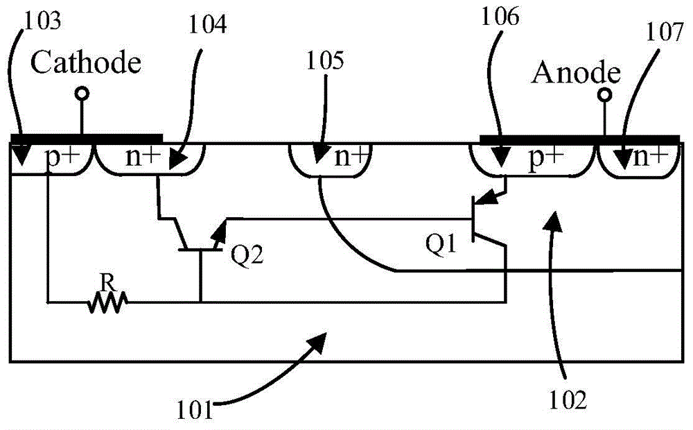
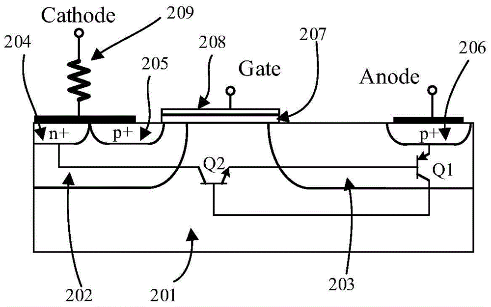
[0021] Such as figure 2 As shown, it is a schematic structural diagram of this example, including a P-type substrate 201, two N-type well regions 202 and 203, two P-type heavily doped regions 205 and 206, an N-type heavily doped region 204, and a gate oxide layer. 207 , polysilicon gate 208 and resistor 209 . Wherein the resistance value of the resistor 209 is relatively small. The two N-type well regions 202 and 203 are located on the P-type substrate 201, the N-type heavily doped region 204 and the first P-type heavily doped region 205 are located on the first N-type well region 202, and the first P-type The heavily doped region 205 is located on the side close to the gate, the gate oxide layer 207 is located on the P-type substrate 201, between the first P-type heavily doped region 205 and the second N-type well region 203, and the second P-type The heavily doped region 206 is located on the second N-type well region 203 . One end of the resistor 209 is connected to the...

Embodiment 2

[0026] Such as Figure 4 As shown, in this example, on the basis of the structure of Embodiment 1, a second N-type heavily doped region 210 is also provided on the second N-type well region 203, and the second N-type heavily doped region 210 is located in the In the second N-type well region 203 , located on the right side of the second P-type heavily doped region 206 , the second N-type heavily doped region 210 and the second P-type heavily doped region 206 together form an anode.

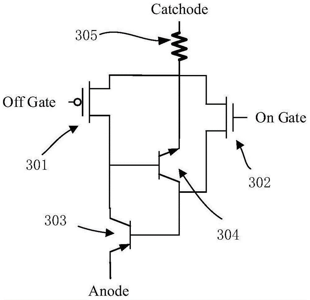
[0027] The working principle of this example is the same as that of Example 1, except that the second N-type heavily doped region 210 is set, which will reduce the gain of the parasitic PNP transistor Q1, improve the ability of the PMOS 301 to turn off the current, and improve the The ability of the device to discharge ESD current.

Embodiment 3

[0029] Such as Figure 5As shown, on the basis of Embodiment 1 of this example, an oxide layer 211 is provided on the P-type substrate 201, and the oxide layer 211 is located on the P-type substrate 201 and between the two N-type well regions 202 and 203. Down.

[0030] The working principle of this example is the same as that of Example 1. The difference is that the setting of the oxide layer 211 reduces the current on the substrate, and the current path is closer to the gate, which will help to improve the hole extraction capability of the PMOS channel, thereby improving the off-current of the PMOS301. The ability to improve the ability of the device to discharge the ESD current.


PUM


Abstract

The invention relates to an electronic technology, and particularly relates to an SCR (Semiconductor Control Rectifier) shut-off device with latching resistant capability. When an ESD (Electronic Static Discharge) pulse is additionally added, an RC (Remote Control) trigger circuit provides a high potential for grid voltage to start an NMOS (N-channel Metal Oxide Semiconductor), so that an SCR is effectively started, and the purpose of current leakage is achieved; after the current of the ESD pulse leaks, the RC trigger circuit provides a low potential for the grid voltage to start a PMOS (P-channel Metal Oxide Semiconductor), the gain of a parasitic NPN transistor is reduced, the condition of latching effect can not be met, and the SCR is effectively shut off, so that the latching effect is prevented from being generated under an electrifying condition. The SCR shut-off device disclosed by the invention is especially suitable for SCR devices used for ESD protection.

Description

technical field [0001] The present invention relates to electronic technology, specifically relates to the electrostatic discharge (ElectroStatic Discharge, ESD for short) protection circuit design technology of semiconductor integrated circuit chips, especially a kind of SCRESD protection device with high latch up immunity that can be turned off. Background technique [0002] In the process of chip production, packaging, testing, storage, and handling, electrostatic discharge is ubiquitous as an inevitable natural phenomenon. With the reduction of the feature size of integrated circuit technology and the development of various advanced technologies, it is more and more common for chips to be damaged by ESD phenomena. Relevant research and investigations have shown that 30% of integrated circuit failure products are caused by electrostatic discharge phenomena. caused. Therefore, it is very important to use high-performance ESD protection devices to protect the internal circ...

Claims


Application Information

Patent Timeline
Patent Type & Authority Patents(China)
IPC IPC(8): H01L27/02
Inventor 乔明马金荣齐钊黄军军曲黎明张波
Owner UNIV OF ELECTRONICS SCI & TECH OF CHINA
Why Eureka
Try Eureka