
Integrated circuit module and packaging assembly thereof

A technology of integrated circuits and components, applied in the field of semiconductor packaging components, can solve problems such as adverse effects on performance, achieve the effects of improving heat dissipation, reducing interconnection resistance, and simplifying design

Active Publication Date: 2014-08-13
SILERGY SEMICON TECH (HANGZHOU) CO LTD
View PDF4 Cites 2 Cited by
  • Summary
  • Abstract
  • Description
  • Claims
  • Application Information

AI Technical Summary

Problems solved by technology

[0006] In view of this, the object of the present invention is to provide an integrated circuit assembly and its packaging assembly, to solve the problem that the electrical connection of multiple electronic devices adversely affects its performance

Method used


Image

  • Integrated circuit module and packaging assembly thereof
  • Integrated circuit module and packaging assembly thereof
  • Integrated circuit module and packaging assembly thereof

Examples


Embodiment Construction

[0054] Various embodiments of the invention will be described in more detail below with reference to the accompanying drawings. In the various drawings, the same elements are denoted by the same or similar reference numerals.

[0055] For the sake of clarity, various parts in the drawings have not been drawn to scale. For simplicity, the component structure obtained after several steps can be described in one figure. Additionally, certain well-known details may be omitted, eg, solder, encapsulant, support material for supporting the lead frame, and / or external frame are not shown in some of the drawings.

[0056] It should be understood that when describing a component structure, when a layer or a region is referred to as being “on” or “over” another layer or another region, it may mean that it is directly on another layer or another region, or on the There are other layers or regions between it and another layer or another region. And, if the device is turned over, the lay...


PUM


Abstract

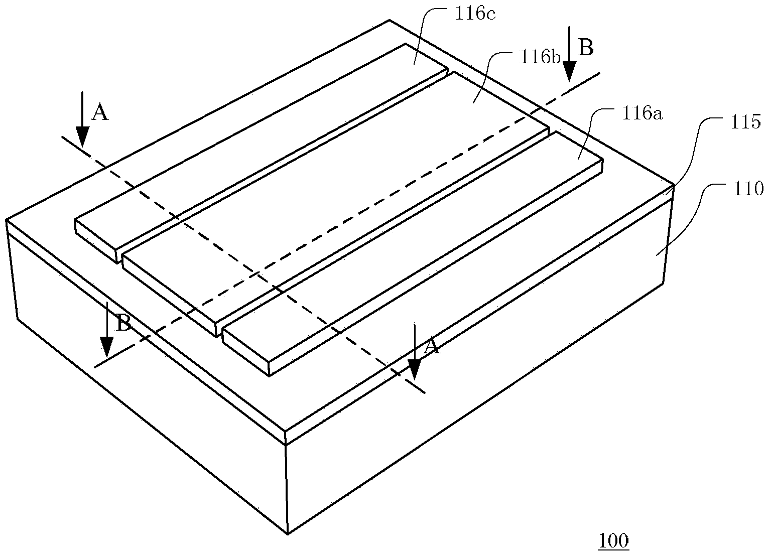
The invention discloses an integrated circuit module and a packaging assembly of the integrated circuit module. The integrated circuit module comprises a semiconductor bare chip, a first insulation layer and i power buses, wherein the semiconductor bare chip comprises a plurality of electronic devices which are divided into m sets, each electronic device comprises n electrodes with different polarities, and m and n are both integers larger than one; the first insulation layer is located on the surface of the semiconductor bare chip; the i power buses comprise a plane extending portion located on the first insulation layer and a plurality of perpendicular channel portions which penetrate through the first insulation layer and are connected with all electrodes of the devices, i is an integer larger than one and smaller than or equal to m*n, one electrode of each device in at least two electronic devices and one electrode of another device in at least two electronic devices are electrically connected through at least one power bus among the i power buses, and each power bus among the i power buses is connected to an external connecting terminal. By the adoption of the integrated circuit module, a lead frame with a finger-shaped lead fin is omitted, so that the design of the lead frame is simplified, the interconnection resistance is reduced, and heat dissipation performance is improved.

Description

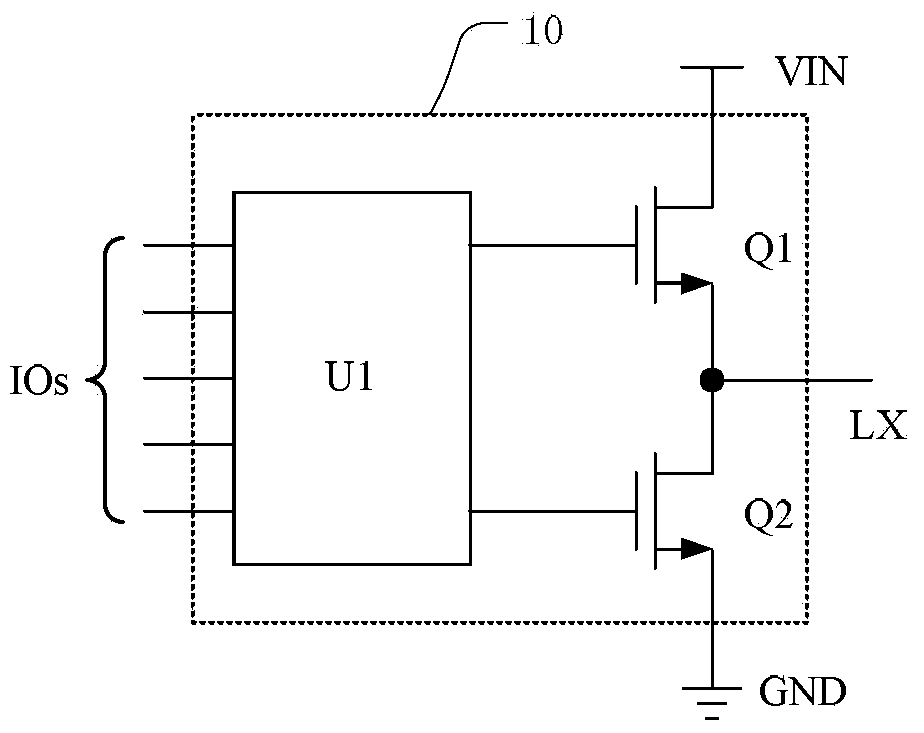
technical field [0001] The present invention relates to a semiconductor packaging assembly, and more particularly to an integrated circuit assembly and packaging assembly applied to a switching regulator. Background technique [0002] Switching regulators, such as DC-DC converters, are used to provide a stable voltage source for a variety of electrical systems. High-efficiency DC-DC converters are especially required for battery management in low-power devices (such as laptops, cell phones, etc.). Switching regulators convert the input DC voltage to a high frequency voltage, and then filter the high frequency output voltage to convert it to a DC output voltage. [0003] figure 1 A circuit schematic of a typical switching regulator 10 is shown. The switching regulator includes a control stage and a power stage. The control stage includes the control chip U1. The power stage includes power devices Q1 and Q2. Power devices are, for example, field effect transistors or bip...

Claims


Application Information

Patent Timeline
Patent Type & Authority Applications(China)
IPC IPC(8): H01L23/495
CPCH01L2924/0002H01L2924/1305H01L2224/16245
Inventor 叶佳明谭小春
Owner SILERGY SEMICON TECH (HANGZHOU) CO LTD
Learn More