A kind of led packaging structure

A technology of LED packaging and sealing layer, applied in electrical components, electrical solid devices, circuits, etc., can solve the problems of high cost, poor yield, small LED lamp beads not making high-density static screens, etc., to achieve a small footprint , the effect of small spacing

Active Publication Date: 2018-02-13
GUANGDONG VTRON TECH CO LTD
View PDF4 Cites 0 Cited by
  • Summary
  • Abstract
  • Description
  • Claims
  • Application Information

AI Technical Summary

Problems solved by technology

But small LED lamp beads are not the key to making high-density static screens
Although traditional discrete devices can be used in the prior art to achieve static display, this solution is point-to-point control through the driver IC, that is, one output channel only controls one LED light-emitting chip, so more driver ICs or increased output channels are required. At the same time, the wiring density and complexity of the PCB board will also increase. More ICs will increase the power consumption of the display screen, and the complex PCB board process will lead to poor yield and high cost, resulting in the entire display Increase in screen cost

Method used


Image

  • A kind of led packaging structure
  • A kind of led packaging structure
  • A kind of led packaging structure

Examples


Embodiment 1

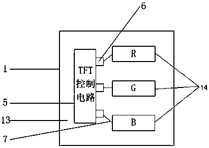
[0023] Such as figure 1 As shown, it is a structural schematic diagram of a specific embodiment of an LED packaging structure according to the present invention. see figure 1 In this specific embodiment, an LED packaging structure includes at least one set of LED light-emitting chips 14, a PCB board 13, and a TFT control circuit module 5 for controlling at least one set of LED light-emitting chips 13, and the TFT control circuit module 5 and at least one set of LED light-emitting chips. The light-emitting chip 14 is packaged on the PCB board 13 to form a COB structure, the TFT control circuit module 5 is provided with electrodes 6 connected to at least one group of LED light-emitting chips 14, and the TFT control circuit module 5 and at least one group of LED light-emitting chips 14 are formed with a package. glue layer.

[0024] In this specific embodiment, the TFT (Thin Film Transistor, Thin Film Transistor) control circuit module 5 is integrated into the LED light-emittin...

Embodiment 2

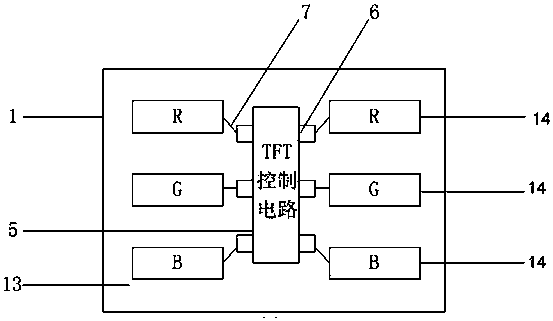
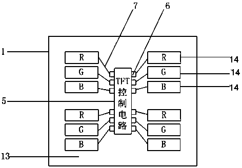
[0033] The difference between this embodiment and Embodiment 1 is that the TFT control circuit module 5 only includes a TFT matrix control circuit, and then the TFT matrix control circuit is directly fabricated on the PCB board 13 and connected with at least one group of LED light-emitting chips, so that the PCB board 13 Possesses functions of TFT control circuit such as Figure 7 shown. Compared with Embodiment 1, this embodiment does not need a substrate for integrating the TFT control circuit module 5, but makes the TFT matrix control circuit on the PCB board 13, thereby reducing the manufacturing process of the TFT matrix control circuit module and improving production. High efficiency reduces the cost of production, and because it is not limited by the substrate, it can more effectively reduce the distance between the TFT control circuit module 5 and the LED light-emitting chip, so as to make full use of the space and increase the arrangement density to achieve higher res...


PUM


Abstract

The invention relates to the field of LED packaging, and more particularly relates to an LED packaging structure capable of realizing static display. It includes at least one set of LED light-emitting chips, a PCB board, and a TFT control circuit module that controls at least one set of LED light-emitting chips. The TFT control circuit module and at least one set of LED light-emitting chips are packaged on the PCB to form a COB structure. The TFT control circuit The module is provided with electrodes connecting at least one group of LED light-emitting chips, and a sealant layer is formed on the TFT control circuit module and at least one group of LED light-emitting chips. In the present invention, the LED lamp bead or the TFT control circuit module in the LED module directly controls the LED light-emitting chip, and controls whether the LED light-emitting chip is lit through the TFT site selection, and ensures continuous power supply through the TFT control circuit module after the site selection is completed. Make the LED chip emit light continuously, and it can realize static display when applied to the display screen.

Description

technical field [0001] The invention relates to the field of LED packaging, and more particularly relates to an LED packaging structure capable of realizing static display. Background technique [0002] In recent years, LED displays have developed rapidly. From the initial large-pitch, low-definition outdoor display to the current small-pitch, ultra-high-definition indoor high-end display, the technical difficulty is constantly escalating, and customers' requirements for display performance are also increasing. The higher the LED, the smaller the LED has become its development trend. But small LED lamp beads are not the key to making high-density static screens. Although traditional discrete devices can be used in the prior art to achieve static display, this solution is point-to-point control through the driver IC, that is, one output channel only controls one LED light-emitting chip, so more driver ICs or increased output channels are required. At the same time, the wiri...

Claims


Application Information

Patent Timeline
Patent Type & Authority Patents(China)
IPC IPC(8): H01L25/16
Inventor 张世诚彭晓林孙婷
Owner GUANGDONG VTRON TECH CO LTD
Why Eureka
Try Eureka