Wafer surface defect feature analysis method and system and wafer surface detect feature classification method and system

A feature analysis and wafer technology, applied in image analysis, image data processing, instruments, etc., can solve the problems of high difficulty in classification of wafer surface defects and high misclassification rate, and achieve improved classification accuracy, high accuracy, and reduced The effect of misclassification

Inactive Publication Date: 2014-08-27
HANS LASER TECH IND GRP CO LTD +1
View PDF3 Cites 31 Cited by
  • Summary
  • Abstract
  • Description
  • Claims
  • Application Information

AI Technical Summary

Problems solved by technology

In addition, because the process of obtaining the wafer image is affected by external factors, there will be more interference areas that do not belong to any defect type
Therefore, the classification of wafer surface defects has problems such as high classification difficulty and high misclassification rate.

Method used


Image

  • Wafer surface defect feature analysis method and system and wafer surface detect feature classification method and system
  • Wafer surface defect feature analysis method and system and wafer surface detect feature classification method and system
  • Wafer surface defect feature analysis method and system and wafer surface detect feature classification method and system

Examples


Embodiment Construction

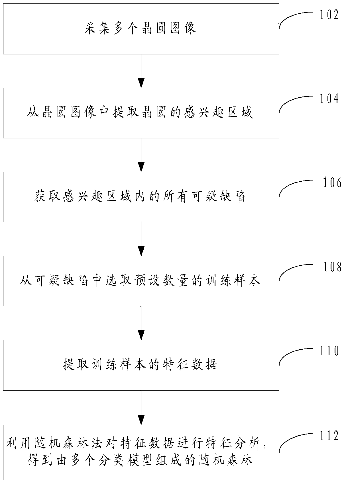
[0042] In order to make the object, technical solution and advantages of the present invention clearer, the present invention will be further described in detail below in conjunction with the accompanying drawings and embodiments. It should be understood that the specific embodiments described here are only used to explain the present invention, not to limit the present invention.

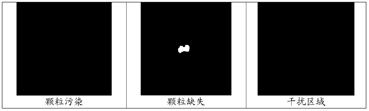
[0043] The surface defects of the wafer mainly include: pinholes, particle contamination, missing particles, and scratches, etc. In addition, there will be an interference area due to the relationship between image quality among the detected defects. Among them, the state of pinholes in the wafer is a small white bright spot; the state of particle pollution is a black area, including large particle pollution and small particle pollution; the state of image loss is a white area; the state of scratches The present state is a white linear area, and the present state of the interference area is a criti...


PUM


Abstract

The invention provides a wafer surface detect feature analysis method. The method comprises the steps that a plurality of wafer images are collected; wafer interesting areas of a wafer are extracted from the wafer images; all suspicious defects in the interesting areas are obtained; a preset number of training samples are selected from the suspicious defects; feature data of the training samples are extracted; feature analysis is conducted on the feature data through the random forest method, and a random forest formed by a plurality of classification models is obtained. By the adoption of the method, the wafer surface defect error classification rate can be reduced, and classification accuracy is improved. The invention further provides a wafer surface detect feature analysis system and a wafer surface detect feature classification method and system.

Description

technical field [0001] The invention relates to the field of semiconductor manufacturing and processing, in particular to a wafer surface defect feature analysis method, system, classification method and system. Background technique [0002] LED wafers are the basic material of semiconductors and the core part of LEDs. The quality of the wafer seriously affects the main photoelectric parameters such as the wavelength, brightness, and forward voltage of the LED, and also affects the efficiency of semiconductor processing. Using the data obtained from defect detection to judge the processing method of the wafer will improve the processing efficiency. The existence of surface defects and the types of defects are various. In addition, because the process of obtaining the wafer image is affected by external factors, many interference areas that do not belong to any defect type will appear. Therefore, the classification of wafer surface defects has problems such as high classif...

Claims


Application Information

Patent Timeline
Patent Type & Authority Applications(China)
IPC IPC(8): G06T7/00
Inventor 舒远李玉廷王光能周蕾米野丁兵高云峰
Owner HANS LASER TECH IND GRP CO LTD
Why Eureka
Try Eureka