A method of making a photodiode

A technology of photodiode and manufacturing method, which is applied to circuits, electrical components, semiconductor devices, etc., can solve the problem of insufficient photodiode responsivity, and achieve the effect of improving responsivity.

Active Publication Date: 2016-05-18
WUHAN TELECOMM DEVICES
View PDF3 Cites 0 Cited by
  • Summary
  • Abstract
  • Description
  • Claims
  • Application Information

AI Technical Summary

Problems solved by technology

[0004] In view of the above problems, the object of the present invention is to provide a method for manufacturing a photodiode, aiming at solving the technical problem that the responsivity of the existing photodiode is not fast enough

Method used


Image

  • A method of making a photodiode
  • A method of making a photodiode
  • A method of making a photodiode

Examples


Embodiment 1

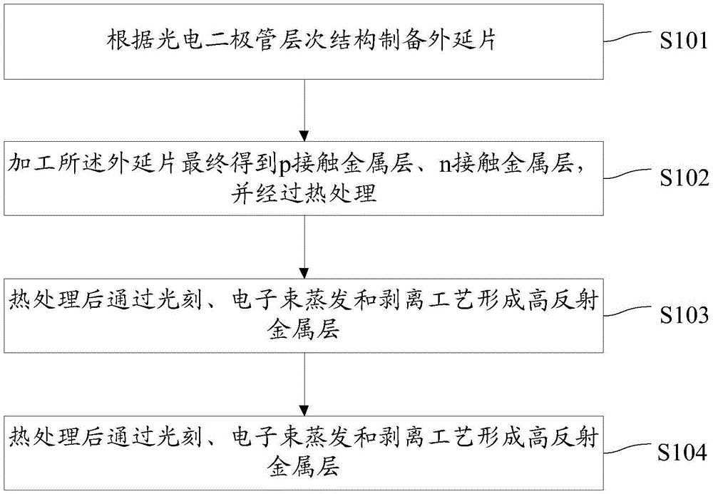
[0020] figure 1 The process flow of the method for manufacturing a photodiode provided by the embodiment of the present invention is shown, and only the parts related to the embodiment of the present invention are shown for convenience of description.

[0021] The fabrication method of the photodiode provided in this embodiment comprises the following steps:

[0022] Step S101 , preparing an epitaxial wafer according to the hierarchical structure of the photodiode.

[0023] Different photodiodes may have epitaxial wafer structures with different levels. Generally, the metal organic chemical vapor deposition method is used to sequentially grow each layer on the InP substrate, and finally the epitaxial wafer is obtained.

[0024] Step S102 , processing the epitaxial wafer to finally obtain a p-contact metal layer and an n-contact metal layer, and undergo heat treatment.

[0025] The specific manufacturing process may be different for different photodiodes, but they all include...

Embodiment 2

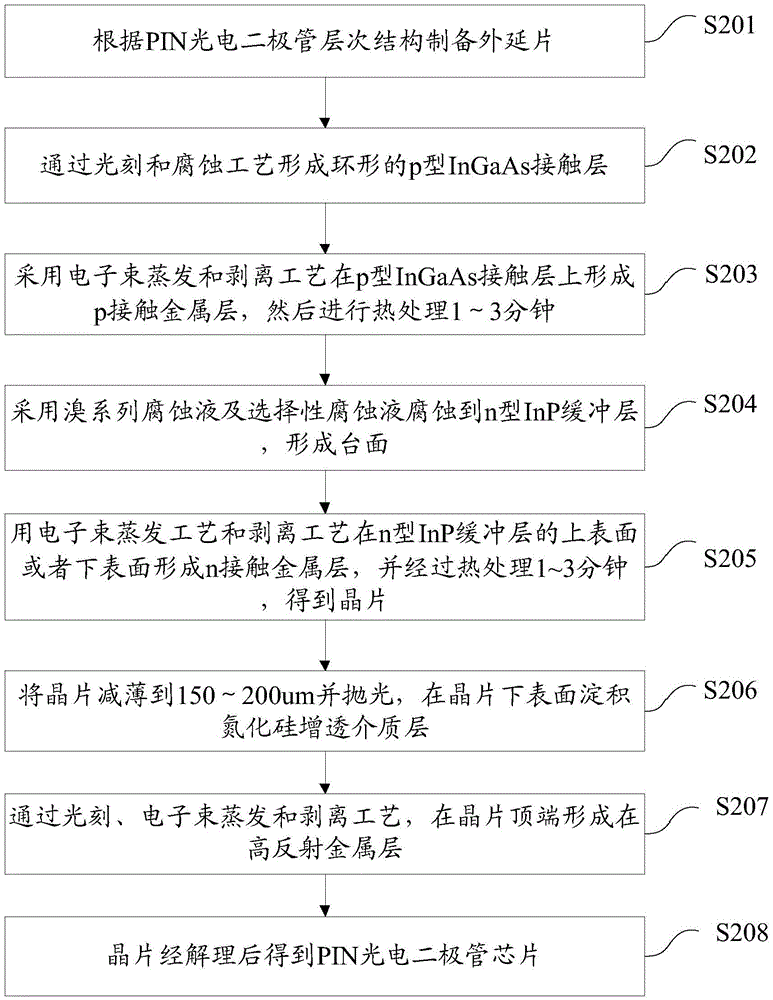
[0030] figure 2 The process flow of the method for manufacturing a photodiode provided by the embodiment of the present invention is shown, and only the parts related to the embodiment of the present invention are shown for convenience of description.

[0031] In this embodiment, a PIN photodiode is taken as an example to specifically describe the method for fabricating the photodiode. Such as figure 2 shown, including the following steps:

[0032] Step S201 , preparing an epitaxial wafer according to the hierarchical structure of the PIN photodiode.

[0033] The PIN photodiode is produced by etching the epitaxial wafer. The epitaxial wafer of the PIN photodiode includes an n-type InP substrate at the bottom layer. Each layer is sequentially grown on the InP substrate by metal organic chemical vapor deposition, including the n-type InP buffer. Layer, I-type InGaAs light absorbing layer, p-type InP window layer, p-type InGaAs contact layer. As an implementation manner, th...

Embodiment 3

[0050] Figure 5 The process flow of the method for manufacturing a photodiode provided by the embodiment of the present invention is shown, and only the parts related to the embodiment of the present invention are shown for convenience of description.

[0051] In this embodiment, an avalanche photodiode is taken as an example to specifically describe the method for fabricating the photodiode. Such as Figure 5 shown, including the following steps:

[0052] Step S501 , preparing an epitaxial wafer according to the hierarchical structure of the avalanche photodiode.

[0053] The avalanche photodiode is produced by etching the epitaxial wafer. The epitaxial wafer of the avalanche photodiode includes an n-type InP substrate at the bottom layer. Various layers are sequentially grown on the InP substrate by metal organic chemical vapor deposition, including n-type InP buffer Layer, I-type InGaAs light absorption layer, n-type InP electric field control layer, n-type InP window l...


PUM

PropertyMeasurementUnit
thicknessaaaaaaaaaa
thicknessaaaaaaaaaa
thicknessaaaaaaaaaa

Abstract

The invention is suitable for chip manufacturing field, and provides a manufacturing method of photo diodes, which comprises the following steps: preparing an epitaxial wafer according to photo diode architecture; machining the epitaxial wafer for finally obtaining a p contact metal layer, an n contact metal layer, and performing thermal treatment; after thermal treatment, forming a high-reflection metal layer through photo-etching, electronic beam evaporating and stripping processes; and obtaining a photo diode chip through cleavage. According to the technical solution of the manufacturing method, after the p contact metal layer and the n contact metal layer are all manufactured, and furthermore all thermal treatments are performed, a high-reflection metal layer is formed. The reflection rate of the high-reflection metal layer can be improved to above 75%, and responsibility of the photo diode is effectively improved.

Description

technical field [0001] The invention belongs to the field of chip manufacturing, in particular to a method for manufacturing a photodiode. Background technique [0002] In optical communication, the detector is required to receive the optical signal, and the responsivity of the detector is usually improved to improve the sensitivity of the detector. In the design of high-speed detectors, in order to increase the working rate of the detector, its bandwidth needs to be increased, so the thickness of the absorption region needs to be reduced, and reducing the absorption region will reduce the detector responsivity. For example, when the thickness of the InGaAs absorption region is reduced to 1um, The responsivity will be reduced to 0.61A / W (1550nm wavelength), and the reduction of responsivity will reduce the sensitivity of the detector. Since the absorption area of ​​the high-speed detector is small, such as a 25-40Gb / s detector, the diameter of the absorption area Usually 5 ...

Claims


Application Information

Patent Timeline
Patent Type & Authority Patents(China)
IPC IPC(8): H01L31/18
CPCH01L31/02161H01L31/184
Inventor 岳爱文胡艳王权兵林玲
Owner WUHAN TELECOMM DEVICES
Why Eureka
Try Eureka