Pixel circuit and display device using the same

A pixel circuit and display device technology, applied to static indicators, instruments, etc., can solve problems such as uneven panel display

Active Publication Date: 2014-09-17
AU OPTRONICS CORP
View PDF5 Cites 12 Cited by
  • Summary
  • Abstract
  • Description
  • Claims
  • Application Information

AI Technical Summary

Problems solved by technology

[0005] The present invention proposes a pixel circuit,

Method used


Image

  • Pixel circuit and display device using the same
  • Pixel circuit and display device using the same
  • Pixel circuit and display device using the same

Examples


Embodiment Construction

[0043] The technical solution of the present invention will be described in detail below in conjunction with the accompanying drawings and specific embodiments to further understand the purpose, solution and effect of the present invention, but it is not intended to limit the scope of protection of the appended claims of the present invention.

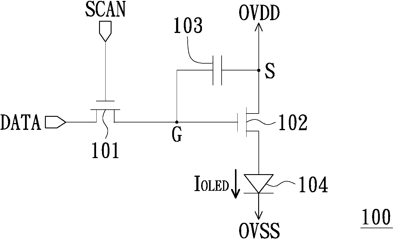
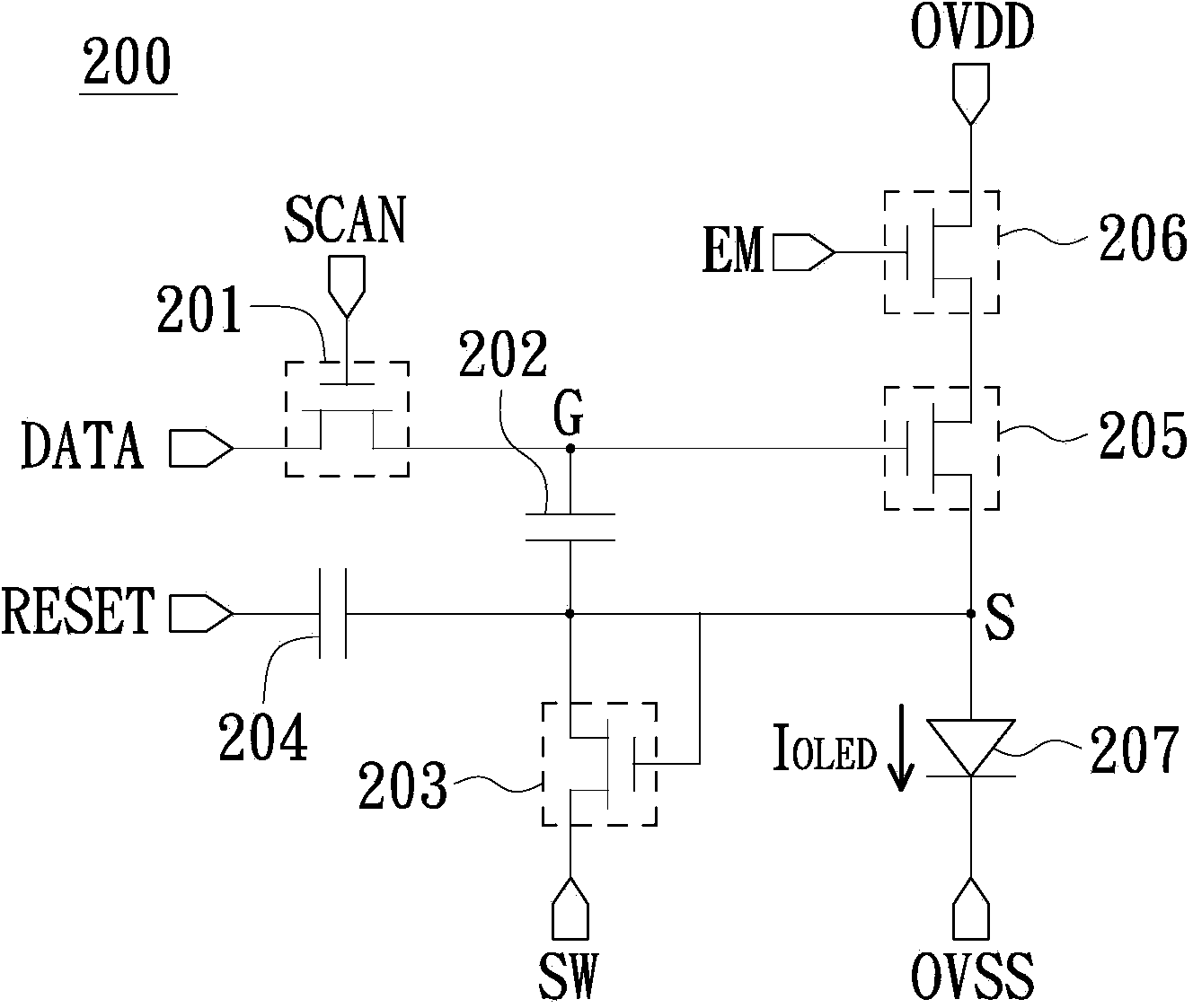
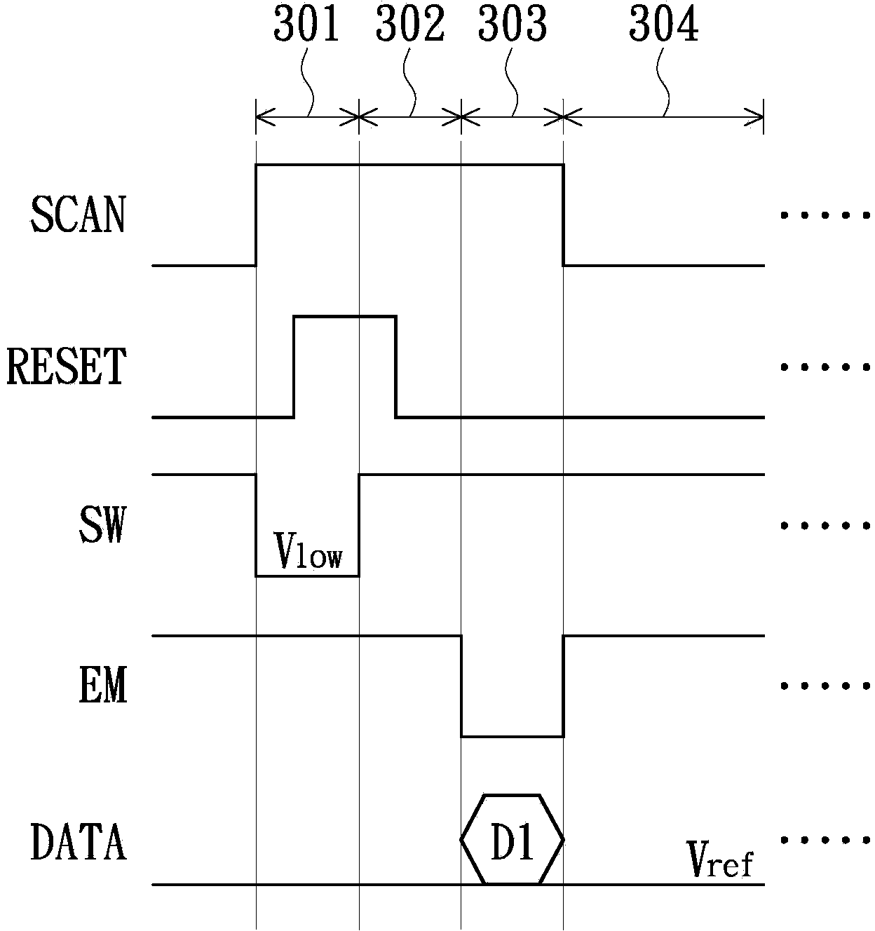
[0044] figure 2 It is a schematic diagram of a pixel circuit according to an embodiment of the present invention. Please refer to figure 2, the pixel circuit 200 is composed of a transistor 201 , a capacitor 202 , a transistor 203 , a capacitor 204 , a transistor 205 , a transistor 206 and a light emitting component 207 . The gate of the transistor 201 is suitable for receiving the scan signal SCAN, and the source / drain of the transistor 201 is suitable for receiving the display data DATA. One end of the capacitor 202 is electrically coupled to the other source / drain of the transistor 201 . The gate of the transistor 203 is electr...


PUM


Abstract

A pixel circuit and a display device using the same are provided. The pixel circuit comprises first to fourth transistors, first and second capacitors and a light emitting assembly. The gate electrode of the first transistor receives a scanning signal; one source/drain electrode of the first transistor receives display data; another source/drain electrode is electrically coupled to the gate electrode of the third transistor and is electrically coupled to one source/drain electrode of the second transistor. The gate electrode and one source/drain electrode of the second transistor receive a reset signal via the second capacitor, and another source/drain electrode receives a switch signal. The gate electrode of the fourth transistor receives an enabling signal; one source/drain electrode is electrically coupled to a first power supply voltage; another source/drain electrode is electrically coupled to the anode of the light emitting assembly through the third transistor. The cathode of the light emitting assembly is electrically coupled to a second power supply voltage which is smaller than the first power supply voltage. The circuit can effectively improve the problems of nonuniform display and material decay of the light emitting assembly so as to provide high-quality display images.

Description

technical field [0001] The present invention relates to the display technology field of an organic light emitting diode, in particular to a pixel circuit of an organic light emitting diode and a display device using the pixel circuit. Background technique [0002] Each pixel circuit in an Organic Light Emitting Diode (OLED) display device generally uses two transistors and a capacitor to control the brightness performance of the OLED. However, the circuit design of existing pixel circuits often causes the problem of uneven panel display, and figure 1 To explain it. [0003] figure 1 It is a schematic diagram of a conventional pixel circuit. Such as figure 1 As shown, the pixel circuit 100 is generally composed of two transistors 101 and 102 , a capacitor 103 and an organic light emitting diode 104 . The gate of the transistor 101 and one source / drain are suitable for receiving the scanning signal SCAN and the display data DATA respectively, and the other source / drain of...

Claims


Application Information

Patent Timeline
IPC IPC(8): G09G3/32G09G3/3233G09G3/3266G09G3/3291
CPCG09G3/3291G09G3/3233G09G3/3258G09G3/3266G09G2300/0819G09G2300/0852G09G2300/0861G09G2310/0248G09G2310/061G09G2320/0233G09G2320/043
Inventor 张华罡施嫚雯罗敬凯黄建中
Owner AU OPTRONICS CORP
Why Eureka
Try Eureka