Array substrate and touch display device

An array substrate and sensing electrode technology, which is applied in the fields of instrumentation, computing, electrical and digital data processing, etc., can solve the problems of weakening the electric field inductive capacitive coupling between the driving electrode and the sensing electrode, increasing the resolution distance, and increasing the center distance, etc. Electrode spacing, increased sensing area, good effect of capacitive coupling

Active Publication Date: 2017-05-17
BOE TECH GRP CO LTD +1
View PDF6 Cites 0 Cited by
  • Summary
  • Abstract
  • Description
  • Claims
  • Application Information

AI Technical Summary

Problems solved by technology

[0003] Compared with the surface mount (Cover lens fully bonded), in the frame mount structure, since there is an air layer between the Cover lens and the Touchsensor, the dielectric constant of the air is significantly smaller than that of other materials (such as LOCA liquid optical glue), which weakens the The electric field induction (that is, capacitive coupling) between the driving electrode and the sensing electrode leads to a significant decrease in the touch signal, sacrificing the original touch performance
In order to enhance the touch signal, the existing method is: simply increase the two-dimensional size (length and width) of a single driving electrode and sensing electrode, and correspondingly increase the center-to-center distance between adjacent electrodes, which leads to consequences Yes: The minimum resolution distance between the two fingers is significantly increased, and the linearity is significantly worse, which greatly affects the overall touch performance

Method used


Image

  • Array substrate and touch display device
  • Array substrate and touch display device
  • Array substrate and touch display device

Examples


Embodiment Construction

[0024] The specific implementation manners of the present invention will be further described in detail below in conjunction with the accompanying drawings and embodiments. The following examples are used to illustrate the present invention, but are not intended to limit the scope of the present invention.

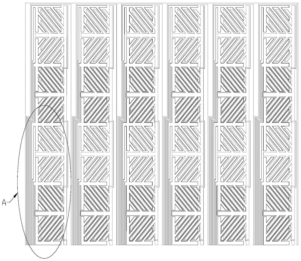
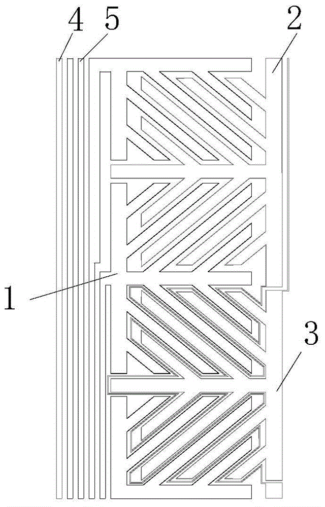
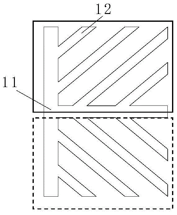
[0025] The present invention provides a display device, which includes an array formed by several driving electrodes and sensing electrodes, and the driving electrodes and sensing electrodes have the same structure, specifically as Figure 1~5 As shown, the structure includes: T-shaped electrode main body (driving electrode main body 11, sensing electrode main body 21) and several electrode branches (driving electrode branch body 12, sensing electrode branch body 22) symmetrically distributed and connected to the electrode main body. , to form two symmetrical parts of the first sub-electrode and the second sub-electrode (such as image 3 The parts shown in the solid and d...


PUM


Abstract

The present invention relates to the field of display technology, and discloses a display device, which includes an array formed by several driving electrodes and sensing electrodes. The driving electrodes and sensing electrodes have the same structure, including: a T-shaped electrode body and symmetrically distributed, and Several electrode branches of the electrode body are connected to form two symmetrical parts, the first sub-electrode and the second sub-electrode. The sensing electrodes include: the first sensing electrode and the second sensing electrode, and two adjacent driving electrodes A first sensing electrode and a second sensing electrode are respectively disposed therebetween, and the electrode branches of the driving electrodes are disposed at gaps between adjacent electrode branches of the sensing electrodes adjacent thereto. Also disclosed is a touch display device. The pattern structure of the sensing layer provided by the present invention and the staggered arrangement of the driving electrodes and the sensing electrodes increase the sensing area between the driving electrodes and the sensing electrodes, and make the capacitive coupling between the electrodes better.

Description

technical field [0001] The present invention relates to the field of display technology, in particular to an array substrate and a touch display device. Background technique [0002] Touch screen is the latest information input device at present. It can realize human-computer interaction simply, conveniently and naturally. It is a brand-new multimedia interactive device. Capacitive touch screen has the advantages of sensitive touch response and multi-touch support. The single-layer ON-CELL capacitive touch screen has the advantages of thinness, low production cost, and integration of touch and display. Among them, the single-layer ON-CELL capacitive touch screen that supports frame stickers is widely favored by end customers because of its advantages such as cheap cover materials, simple process, and easy rework. [0003] Compared with the surface mount (Cover lens fully bonded), in the frame mount structure, since there is an air layer between the Cover lens and the Touchs...

Claims


Application Information

Patent Timeline
Patent Type & Authority Patents(China)
IPC IPC(8): G06F3/044
CPCG06F2203/04107G06F3/0443G06F3/0448G06F3/044
Inventor 叶本银柳皓笛李亮
Owner BOE TECH GRP CO LTD
Why Eureka
Try Eureka