Transistor, stacked transistor and radio frequency switch chip

A transistor, the same technology, applied in the field of stacked transistors and RF switch chips, can solve the problems of inability to insert loss and isolation optimization, and achieve the effect of reducing the trace area, reducing parasitic capacitance and parasitic resistance, and improving isolation.

Pending Publication Date: 2018-12-18
GUANGDONG UNIV OF TECH
View PDF0 Cites 0 Cited by
  • Summary
  • Abstract
  • Description
  • Claims
  • Application Information

AI Technical Summary

Problems solved by technology

However, this kind of packaging optimization only reduces the loss and coupling in the packaging process, and cannot fundamentally optimize the insertion loss and isolation

Method used


Image

  • Transistor, stacked transistor and radio frequency switch chip
  • Transistor, stacked transistor and radio frequency switch chip
  • Transistor, stacked transistor and radio frequency switch chip

Examples


Embodiment Construction

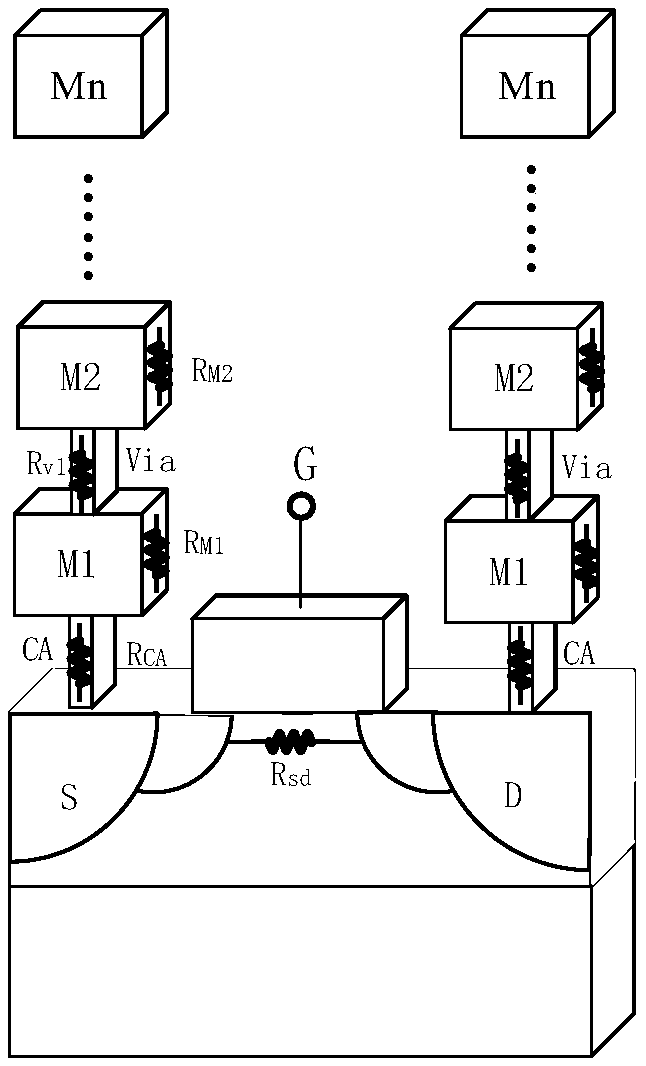
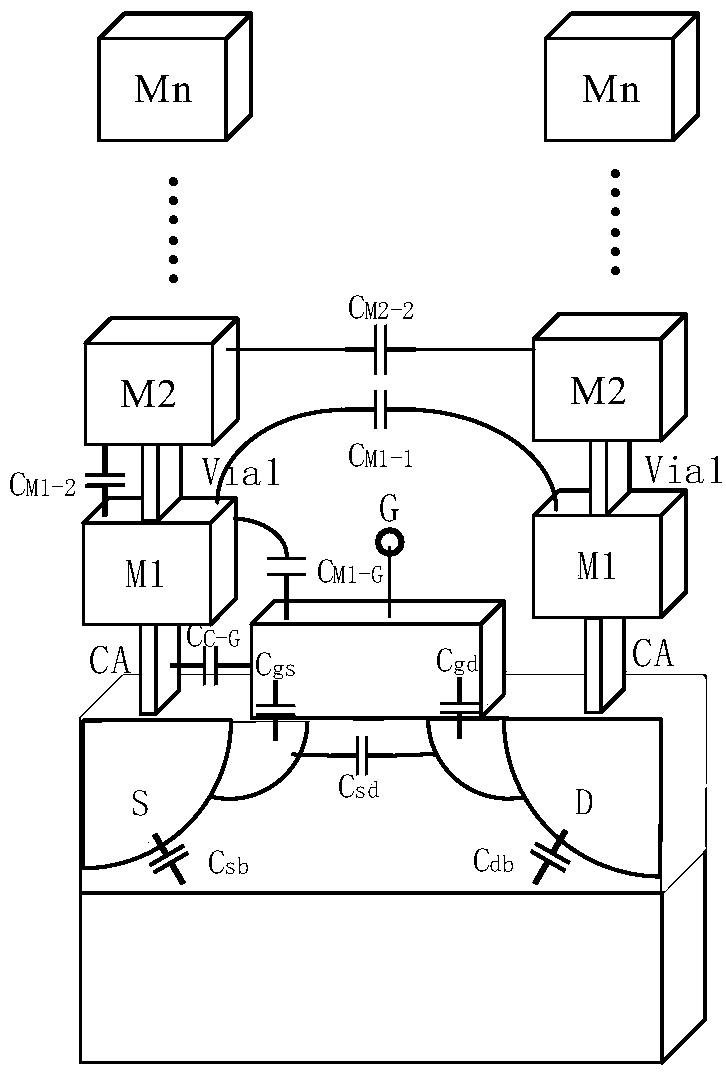
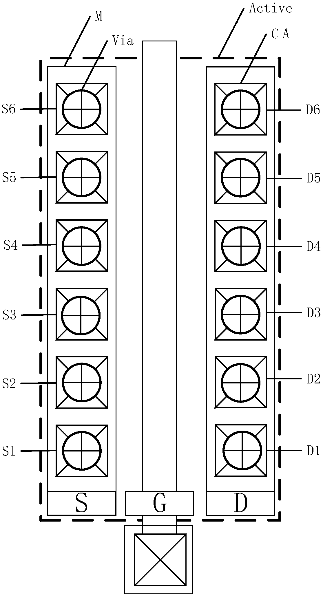
[0032] The core of this application is to provide a transistor, which reduces the area of ​​metal wiring in the metal layer inside the chip by completely staggering the connection of each metal layer on the source region and the drain region of the transistor, from the root of the circuit design Coupling is reduced, insertion loss is effectively reduced, and isolation is improved; another core of the present application is to provide a stacked transistor and a radio frequency switch chip, which also have the above beneficial effects.

[0033] In order to make the purposes, technical solutions and advantages of the embodiments of the present application clearer, the technical solutions in the embodiments of the present application will be clearly and completely described below in conjunction with the drawings in the embodiments of the present application. Obviously, the described embodiments It is a part of the embodiments of this application, not all of them. Based on the embo...


PUM


Abstract

A transistor is disclosed and includes a source region and a drain region parallel to each other in the horizontal direction, A source region and a drain region are provided with a first predeterminednumber of metal layers, wherein each metal layer is stacked and arranged, and the source region and the drain region are respectively connected with the first metal layer through a second predetermined number of vias, wherein each metal layer belonging to the source region is connected with each other through at least one first via; Each metal layer belonging to the drain region is connected witheach other through at least one second via hole; Wherein, in the same metal layer, the first via hole and the second via hole are not arranged at relative positions; By completely staggered the connection of each metal layer on the source region and the drain region, the transistor reduces the metal trace area in the metal layer inside the chip, reduces the coupling from the root cause of the circuit design, effectively reduces the insertion loss and improves the isolation degree. The invention also discloses a stacked transistor and a radio frequency switch chip, which also has the beneficial effects mentioned above.

Description

technical field [0001] The present application relates to the technical field of electronic components, in particular to a transistor, and also to a stacked transistor and a radio frequency switch chip. Background technique [0002] With the development of science and technology, the RF switches used in smartphones are playing an increasingly important role in the design of front-end modules. On the one hand, modern smartphones are constantly pursuing high-speed data transmission and integrating mobile Communication technology; on the other hand, due to the constant pursuit of multi-functionality of smartphones, many other wireless non-cellular communication services are provided, such as FM radio / mobile TV, global positioning system, Bluetooth, wireless local area network and radio frequency tags, etc., among which , the key component that ensures support for so many frequency bands and operating modes in these small devices is the RF switch. For RF switches, the parameter...

Claims


Application Information

Patent Timeline
Patent Type & Authority Applications(China)
IPC IPC(8): H01L29/78H01L21/768H01L25/07H03K17/687
CPCH01L29/78H01L21/768H01L25/073H03K17/687
Inventor 钟立平张志浩章国豪
Owner GUANGDONG UNIV OF TECH
Why Eureka
Try Eureka