Gate drive circuit and display panel and display device comprising same
A gate drive circuit and display panel technology, applied in static indicators, electrical digital data processing, instruments, etc., can solve the problems of increased parasitic capacitance, increased load capacitance, and affecting the overall performance of touch electrodes, achieving good performance Effect
- Summary
- Abstract
- Description
- Claims
- Application Information
AI Technical Summary
Problems solved by technology
Method used
Image


Examples
Embodiment 1
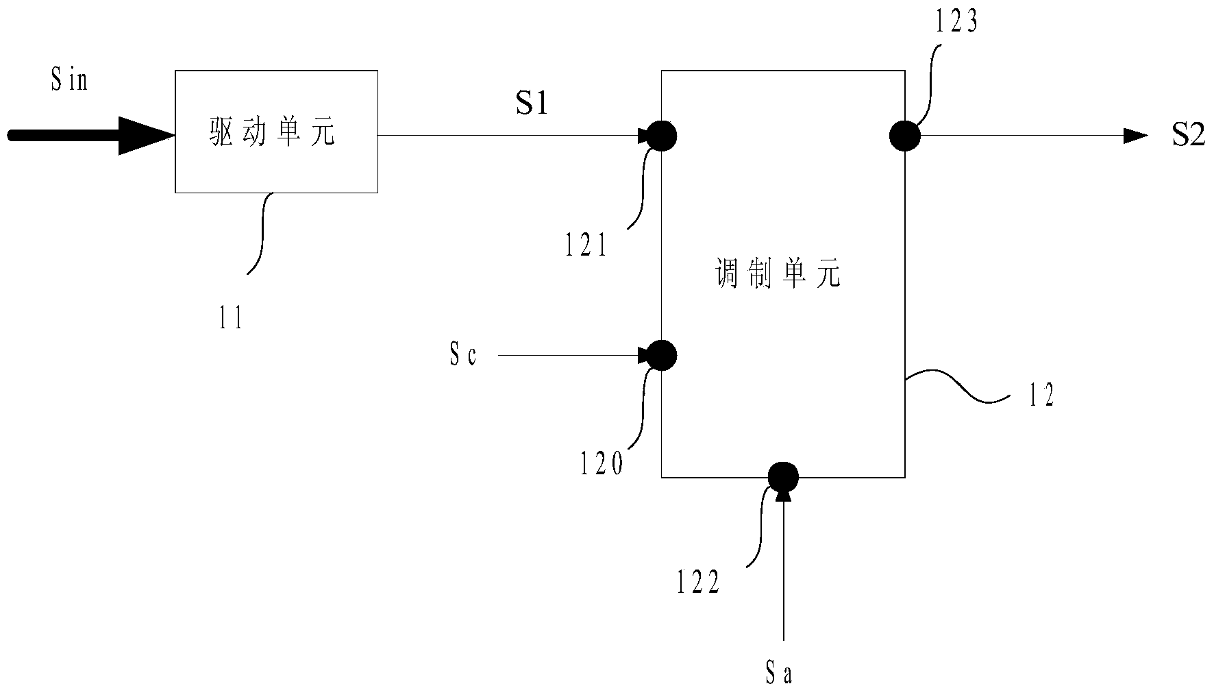
[0037] This embodiment provides a gate drive circuit for a display panel with a self-capacitive touch function, such as image 3As shown, the driving circuit includes: a driving unit 11, configured to receive a plurality of input signals Sin, generate and output a first gate signal S1; a modulation unit 12, including a control terminal 120, a first input terminal 121, a second input terminal 122 and output terminal 123; wherein, the first input terminal 121 receives the first grid signal S1, the second input terminal 122 receives the modulation signal Sa, the control terminal 120 receives the control signal Sc, and the output terminal 123 outputs the second grid signal S2 . The modulation unit 12 selects whether to modulate the first gate signal S1 through the modulation signal Sc according to the received control signal Sc, and outputs the second gate signal S2, so as to reduce the load of the self-capacitance.
[0038] Wherein, the first gate signal S1 is an original gate d...
Embodiment 2
[0043] This embodiment is a refinement of Embodiment 1.
[0044] Specifically, such as Figure 5 As shown, the modulation unit 12 may include a thin film transistor 124, the control terminal 120 of the modulation unit 12 is the gate of the thin film transistor 124, the first input terminal 121 of the modulation unit 12 is coupled to the output terminal 123 of the modulation unit 12, and the modulation unit 12 The second input terminal 122 of the TFT 124 is the first pole of the thin film transistor 124 , and the second pole of the thin film transistor 124 is coupled to the output terminal 123 of the modulation unit 12 . Wherein, coupling may mean direct electrical connection or indirect electrical connection.
[0045] Here, the first pole and the second pole of the thin film transistor 124 are its source and drain respectively, and which one is the source and which is the drain depends on whether the type of the thin film transistor 124 is P-type or N-type, which is not limit...
Embodiment 3
[0049] This embodiment is also a detailed refinement of the first embodiment.
[0050] Such as Figure 6a As shown, the modulation unit 12 may further specifically include a gating circuit 125 and an adding circuit 126, the gating circuit 125 receives the control signal Sc through the control terminal 120 of the modulation unit 12, and receives the modulation signal through the second input terminal 122 of the modulation unit 12 Sa, and output the modulated signal Sa to the addition circuit 126 when the control signal Sc is valid. The addition circuit 126 receives the first gate signal S1 through the first input terminal 121 of the modulation unit 12, and superimposes the modulation signal Sa output by the gating circuit 12 with the first gate signal S1, and passes the output terminal of the modulation unit 12 123 outputs the second gate signal S2.
[0051] This embodiment presents a specific optional structure of the modulating unit 12, so that when the display panel needs ...
PUM
 Abstract
Description
Claims
Application Information
 - Generate Ideas
- Intellectual Property
- Life Sciences
- Materials
- Tech Scout
- Unparalleled Data Quality
- Higher Quality Content
- 60% Fewer Hallucinations
Browse by: Latest US Patents, China's latest patents, Technical Efficacy Thesaurus, Application Domain, Technology Topic, Popular Technical Reports.
© 2025 PatSnap. All rights reserved.Legal|Privacy policy|Modern Slavery Act Transparency Statement|Sitemap|About US| Contact US: help@patsnap.com