Three-dimensional integrated circuit on-chip network routing method and system thereof

An integrated circuit and network-on-chip technology, applied in the field of on-chip network routing of three-dimensional integrated circuits, can solve the problems of on-chip network communication performance, turn to limit low system overhead, etc., and achieve the effects of avoiding additional overhead, improving fairness, and high communication performance.

Active Publication Date: 2014-10-08
INST OF COMPUTING TECH CHINESE ACAD OF SCI
View PDF3 Cites 13 Cited by
  • Summary
  • Abstract
  • Description
  • Claims
  • Application Information

AI Technical Summary

Problems solved by technology

[0007] The purpose of the present invention is to provide a routing method and system for a three-dimensional integrated circuit on-chip network to solve the conflicting problems of on-chip network communication performance, steering restrictions and lower system overhead in the prior art

Method used


Image

  • Three-dimensional integrated circuit on-chip network routing method and system thereof
  • Three-dimensional integrated circuit on-chip network routing method and system thereof
  • Three-dimensional integrated circuit on-chip network routing method and system thereof

Examples


Embodiment Construction

[0048] The present invention will be described in detail below in conjunction with the accompanying drawings and specific embodiments, but not as a limitation of the present invention.

[0049] The present invention will be further described below in conjunction with the accompanying drawings and specific embodiments.

[0050] The object of the present invention is to provide a routing method for a three-dimensional integrated circuit on-chip network guided by a fair steering model. It can balance high communication performance and low system overhead on a three-dimensional integrated circuit on-chip network.

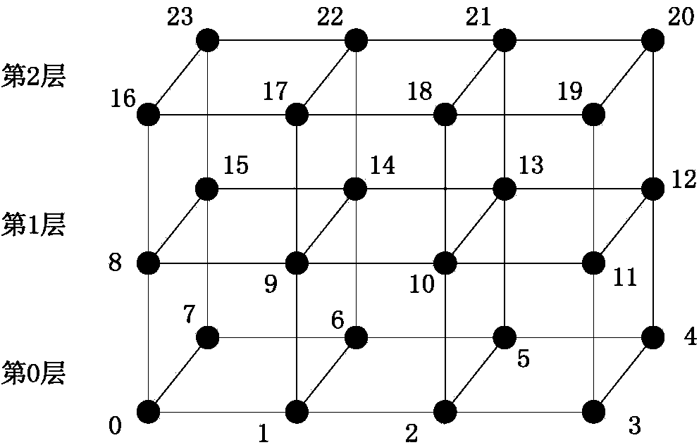
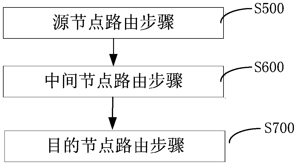
[0051] The invention provides a routing method of a three-dimensional integrated circuit on-chip network guided by a fair steering model, generally speaking, a one-way communication process in which a source node routes data packets to a destination node. Define the source node as S (Source) node, and the destination node as D (Destination) node. Key points of the pre...


PUM


Abstract

The invention discloses a three-dimensional integrated circuit on-chip network routing method. According to the method, a three-dimensional steering model is adopted for routing guidance, a port selection mechanism is adopted for selection of a legal output port, and a data packet is routed in a unidirectional manner from a source node to a destination mode. The three-dimensional steering model is a parity-based steering model, an X-Y plane or an X-Z plane or a Y-Z plane of a three-dimensional scene is used as the datum plane, a routing path between the source node and the destination mode is mapped to the datum plane, and steering limiting is performed on the datum plane by adoption of an inter-layer illegal steering principle of a device layer and a corresponding supplementary principle. The invention further discloses a three-dimensional integrated circuit on-chip network routing system.

Description

technical field [0001] The invention relates to the design field of integrated circuits, in particular to a three-dimensional integrated circuit on-chip network routing method guided by a fair steering model. Background technique [0002] Three-dimensional integration technology is a packaging technology that stacks different device layers of a chip and vertically integrates them together. The title of the packaging technology in the journal is: "proceedings of the IEEE, Volume: 89, Issue: 5, 2001, pp.602-633.", and the title of the document is: "3-D ICs: a novel chip design for improving deep- Submicrometer interconnect performance and systems-on-chip integration," authored by: Banerjee K. et al., disclosed that this technology can shorten the physical connection length in the chip and reduce system delay and power consumption. figure 1 It is a schematic diagram of a simple 4*2*3 three-dimensional chip-on-chip network, and the topology is a three-dimensional Mesh structure...

Claims


Application Information

Patent Timeline
Patent Type & Authority Applications(China)
IPC IPC(8): H04L12/771H04L12/935H04L45/60H04L49/111
Inventor 周君李华伟李晓维
Owner INST OF COMPUTING TECH CHINESE ACAD OF SCI
Why Eureka
Try Eureka