

Internal plasma grid applications for semiconductor fabrication
A plasma and ion technology, applied in the field of plasma grids, can solve problems such as difficult to achieve multiple purposes
- Summary
- Abstract
- Description
- Claims
- Application Information
AI Technical Summary
Problems solved by technology
Method used
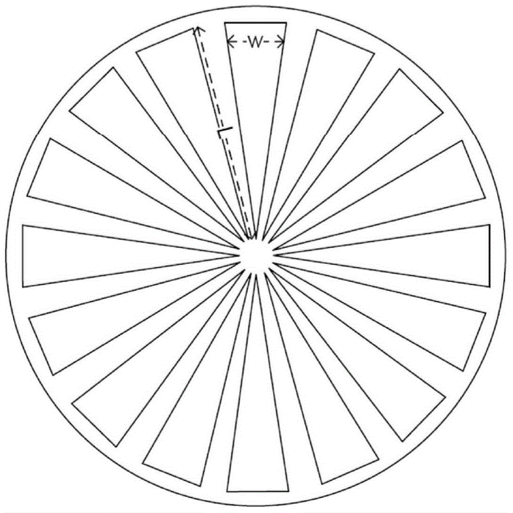
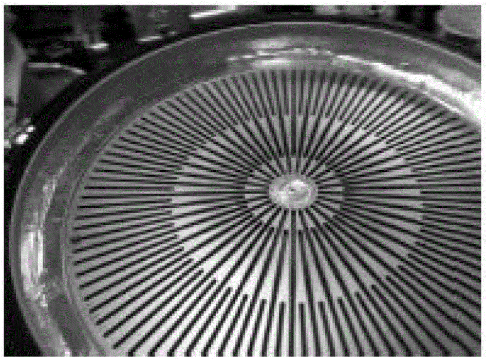
Image

Examples
Embodiment Construction
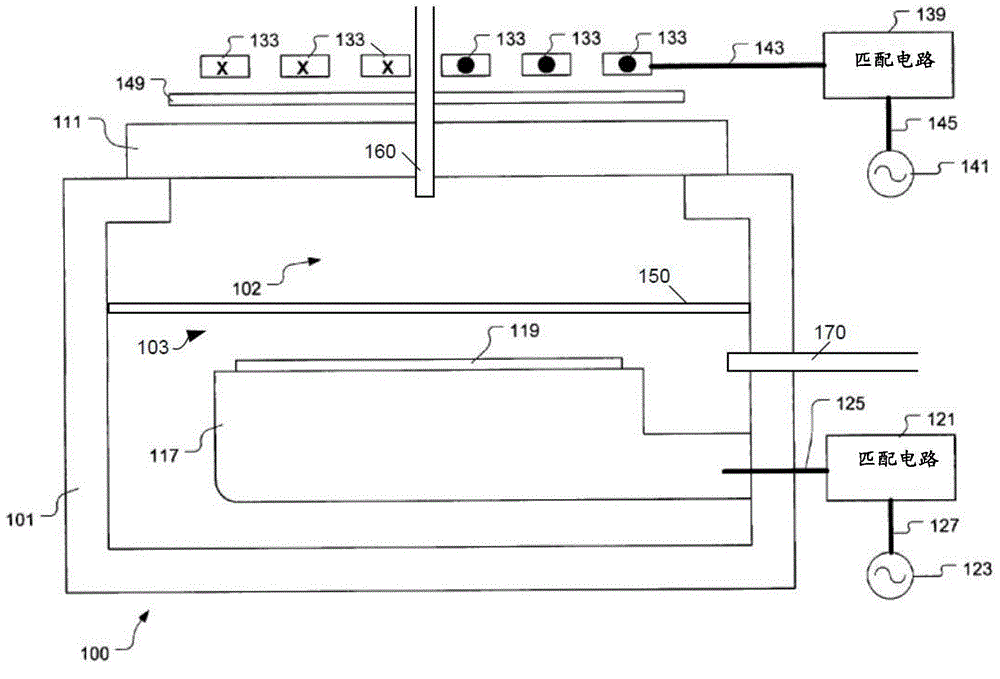
[0043] In this specification, the terms "semiconductor wafer," "wafer," "substrate," "wafer substrate," and "partially fabricated integrated circuit" are used interchangeably. It will be understood by those of ordinary skill in the art that the term "partially fabricated integrated circuit" may refer to devices on a semiconductor wafer during any of the different stages of integrated circuit fabrication on the semiconductor wafer. The following detailed description assumes that the present invention is implemented on a wafer. However, the present invention is not limited thereto. Workpieces can be formed in a variety of shapes, sizes and materials.
[0044] In the following description, numerous specific details are set forth in order to provide a thorough understanding of the present invention. However, the present invention may be practiced without some or all of these specific details. In other instances, well known process operations have not been described in detail in...
PUM
 Abstract
Description
Claims
Application Information