Multi-Level semiconductor package
A semiconductor and bonding layer technology, applied in semiconductor devices, semiconductor/solid-state device manufacturing, semiconductor/solid-state device components, etc., can solve problems such as interconnection layout that limits electrical conductivity and thermal conductivity performance
- Summary
- Abstract
- Description
- Claims
- Application Information
AI Technical Summary
Problems solved by technology
Method used
Image

Examples
Embodiment Construction
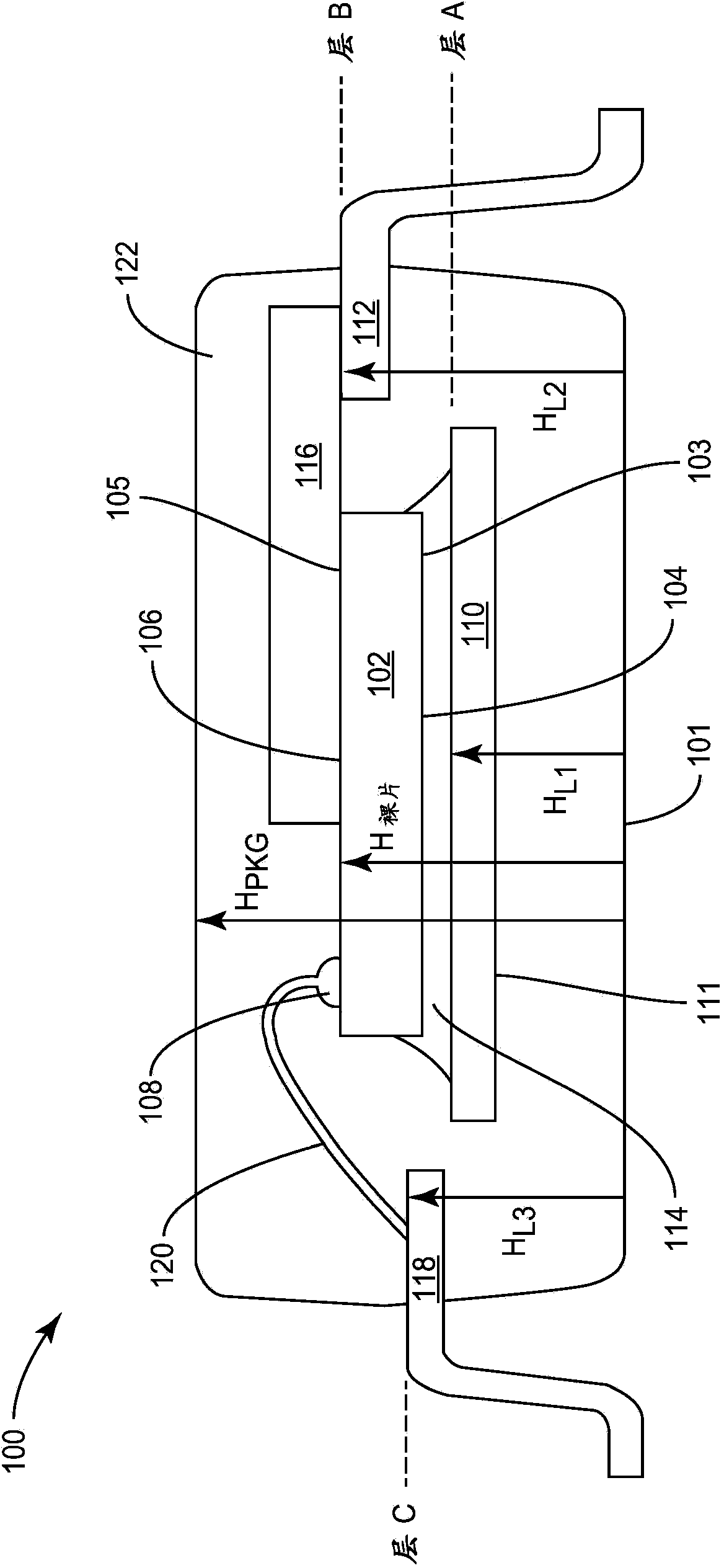
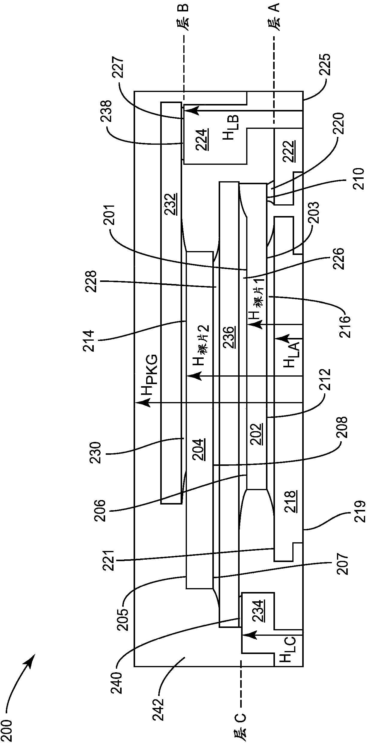
[0015] Embodiments described herein provide a semiconductor package having leads terminated at different layers in the package. At least one connector is included in the package for connecting the one or more semiconductor die electrodes to leads that terminate at the same layer in the package as the connector. Thus, the connector can have a single continuous planar structure with leads extending to the planar connector, rather than a connector that has to bend down towards the same base layer of the package where typically all of the package's leads terminate here. Multiple connectors may be provided having a single continuous planar structure so that multiple die electrodes may be connected to different package leads at multiple levels in the package, each level being arranged generally planarly. Providing leads at different layers in a semiconductor package, and using a single continuous planar structure of connectors for electrode-to-lead connections of the die, improves ...
PUM
 Abstract
Description
Claims
Application Information
 - R&D
- Intellectual Property
- Life Sciences
- Materials
- Tech Scout
- Unparalleled Data Quality
- Higher Quality Content
- 60% Fewer Hallucinations
Browse by: Latest US Patents, China's latest patents, Technical Efficacy Thesaurus, Application Domain, Technology Topic, Popular Technical Reports.
© 2025 PatSnap. All rights reserved.Legal|Privacy policy|Modern Slavery Act Transparency Statement|Sitemap|About US| Contact US: help@patsnap.com